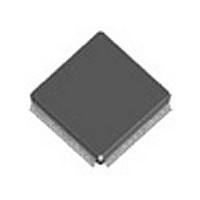
ADSP-2196MBST-140 Analog Devices Inc, ADSP-2196MBST-140 Datasheet - Page 28

ADSP-2196MBST-140
Manufacturer Part Number
ADSP-2196MBST-140
Description
IC DSP CONTROLLER 16BIT 144LQFP
Manufacturer
Analog Devices Inc
Series
ADSP-21xxr
Type
Fixed Pointr
Datasheet
1.ADSP-2196MKSTZ-160.pdf
(68 pages)
Specifications of ADSP-2196MBST-140
Rohs Status
RoHS non-compliant
Interface
Host Interface, SPI, SSP, UART
Clock Rate
140MHz
Non-volatile Memory
ROM (48 kB)
On-chip Ram
40kB
Voltage - I/o
3.30V
Voltage - Core
2.50V
Operating Temperature
-40°C ~ 85°C
Mounting Type
Surface Mount
Package / Case
144-LQFP
Device Core Size
16b
Format
Fixed Point
Clock Freq (max)
140MHz
Mips
140
Device Input Clock Speed
140MHz
Ram Size
40KB
Program Memory Size
48KB
Operating Supply Voltage (typ)
2.5/3.3V
Operating Supply Voltage (min)
2.37V
Operating Supply Voltage (max)
2.63/3.6V
Operating Temp Range
-40C to 85C
Operating Temperature Classification
Industrial
Mounting
Surface Mount
Pin Count
144
Package Type
LQFP
Lead Free Status / Rohs Status
Not Compliant
Available stocks
Company
Part Number
Manufacturer
Quantity
Price
Company:
Part Number:
ADSP-2196MBST-140
Manufacturer:
ON
Quantity:
12 000
ADSP-2196
External Port Write Cycle Timing
Table 11
The external port lets systems extend read/write accesses in three ways: waitstates, ACK input, and combined waitstates
and ACK. To add waits with ACK, the DSP must see ACK low at the rising edge of EMI clock. ACK low causes the DSP
to wait, and the DSP requires two EMI clock cycles after ACK goes high to finish the access. For more information, see
the External Port chapter in the ADSP-219x/2191 DSP Hardware Reference
Table 11. External Port Write Cycle Timing
1
2
3
4
28
t
These are preliminary timing parameters that are based on worst-case operating conditions.
The pad loads for these timing parameters are 20 pF.
EMI clock is the external port clock that is generated from the EMI clock ratio. This signal is not available on an external pin, but (roughly) corresponds
to HCLK (at similar clock ratios).
Parameter
Switching Characteristics
t
t
t
t
t
t
t
t
t
t
t
t
t
Timing Requirement
t
HCLK
CWA
CSWS
AWS
AKS
WSCS
WSA
CWD
WW
CDA
CDD
DSW
DHW
DHW
AKW
is the peripheral clock period.
and
This information applies to a product under development. Its characteristics and specifications are subject to change with-
out notice. Analog Devices assumes no obligation regarding future manufacturing unless otherwise agreed to in writing.
Figure 14
Description
EMI
Chip select asserted to WR de-asserted delay
Address valid to WR setup and delay
ACK asserted to EMI clock high delay
WR de-asserted to chip select de-asserted
WR de-asserted to address invalid
EMI clock low to WR de-asserted delay
WR strobe pulsewidth
WR to data enable access delay
WR to data disable access delay
Data valid to WR de-asserted setup
WR de-asserted to data invalid hold time; wt_hold=0
WR de-asserted to data invalid hold time; wt_hold=1
ACK strobe pulsewidth
4
clock low to WR asserted delay
describe external port write operations.
1, 2, 3
For current information contact Analog Devices at 800/262-5643
Min
4.3
4.9
6.0
4.8
4.5
2.5
t
1.5
3.3
t
3.4
t
10.0
HCLK
HCLK
HCLK
–0.5
–1.4
+3.4
September 2001
Max
2.8
6.5
7.0
7.0
6.6
2.7
4.1
7.4
t
7.4
t
HCLK
HCLK
+4.8
+7.4
REV. PrA
Unit
ns
ns
ns
ns
ns
ns
ns
ns
ns
ns
ns
ns
ns
ns


