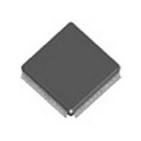
ADSP-2196MBST-140 Analog Devices Inc, ADSP-2196MBST-140 Datasheet - Page 52

ADSP-2196MBST-140
Manufacturer Part Number
ADSP-2196MBST-140
Description
IC DSP CONTROLLER 16BIT 144LQFP
Manufacturer
Analog Devices Inc
Series
ADSP-21xxr
Type
Fixed Pointr
Datasheet
1.ADSP-2196MKSTZ-160.pdf
(68 pages)
Specifications of ADSP-2196MBST-140
Rohs Status
RoHS non-compliant
Interface
Host Interface, SPI, SSP, UART
Clock Rate
140MHz
Non-volatile Memory
ROM (48 kB)
On-chip Ram
40kB
Voltage - I/o
3.30V
Voltage - Core
2.50V
Operating Temperature
-40°C ~ 85°C
Mounting Type
Surface Mount
Package / Case
144-LQFP
Device Core Size
16b
Format
Fixed Point
Clock Freq (max)
140MHz
Mips
140
Device Input Clock Speed
140MHz
Ram Size
40KB
Program Memory Size
48KB
Operating Supply Voltage (typ)
2.5/3.3V
Operating Supply Voltage (min)
2.37V
Operating Supply Voltage (max)
2.63/3.6V
Operating Temp Range
-40C to 85C
Operating Temperature Classification
Industrial
Mounting
Surface Mount
Pin Count
144
Package Type
LQFP
Lead Free Status / Rohs Status
Not Compliant
Available stocks
Company
Part Number
Manufacturer
Quantity
Price
Company:
Part Number:
ADSP-2196MBST-140
Manufacturer:
ON
Quantity:
12 000
ADSP-2196
Output Drive Currents
Figure 27
drivers of the ADSP-2196. The curves represent the current
drive capability of the output drivers as a function of output
voltage.
Power Dissipation
Total power dissipation has two components, one due to
internal circuitry and one due to the switching of external
output drivers. Internal power dissipation is dependent on
the instruction execution sequence and the data operands
involved. Using the current-versus-operation information
in
internal power supply (V
application, according to the formula in
Table 23. ADSP-2196 Operation Types Versus Input Current
1
2
3
4
5
6
Figure 28. I
The external component of total power dissipation is caused
by the switching of output pins. Its magnitude depends on:
• The number of output pins that switch during each cycle
• The maximum frequency at which they can switch (f)
52
Test conditions: V
PLL, Core, peripheral clocks, and CLKIN are disabled.
PLL is enabled and Core and peripheral clocks are disabled.
Core CLK is disabled and peripheral clock is enabled. This is a power- down interrupt mode. The timer can be used to generate an interrupt to enable the
Core clock.
All instructions execute from internal memory. 100% of the instructions are MAC with dual operand addressing, with changing data fetched using a linear
address sequence, and 50% of the instructions move data from PM to a data register.
All instructions execute from internal memory. 50% of the instructions are repeat MACs with dual operand addressing, with changing data fetched using
a linear address sequence.
Activity
Power down
Idle 1
Idle 2
Typical
Peak
(O)
Table
6
3
4
5
I
23, designers can estimate the ADSP-2196’s
DDINT
This information applies to a product under development. Its characteristics and specifications are subject to change with-
out notice. Analog Devices assumes no obligation regarding future manufacturing unless otherwise agreed to in writing.
shows typical I-V characteristics for the output
DDINT
2
DD
=
= 2.50 V; HCLK (peripheral clock) frequency = CCLK/2 (core clock/2) frequency; T
Calculation
%Peak
DDINT
I
DD-PEAK
) input current for a specific
For current information contact Analog Devices at 800/262-5643
Core
0
0
0
95
112
+
%Typical
Figure
28.
CCLK = 80 MHz
I
DD-TYPICAL
I
DD
(mA)
Peripheral
0
3
30
30
30
1
Figure 27. ADSP-2196 Typical Drive Currents
+
• Their load capacitance (C)
• Their voltage swing (V
and is calculated by the formula in
%Idle
I
DD-IDLE
Core
0
0
0
184
215
+
%Powerdown
AMB
DD
= 25 ºC.
)
CCLK = 160 MHz
I
September 2001
DD
Figure
(mA)
I
DD-PWRDWN
Peripheral
0
5
60
60
60
1
29.
REV. PrA


