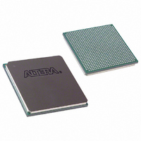
EP3C120F780C8 Altera, EP3C120F780C8 Datasheet - Page 63

EP3C120F780C8
Manufacturer Part Number
EP3C120F780C8
Description
IC CYCLONE III FPGA 119K 780FBGA
Manufacturer
Altera
Series
Cyclone® IIIr
Datasheets
1.EP3C5F256C8N.pdf
(5 pages)
2.EP3C5F256C8N.pdf
(34 pages)
3.EP3C5F256C8N.pdf
(66 pages)
4.EP3C5F256C8N.pdf
(14 pages)
5.EP3C5F256C8N.pdf
(76 pages)
Specifications of EP3C120F780C8
Number Of Logic Elements/cells
119088
Number Of Labs/clbs
7443
Total Ram Bits
3981312
Number Of I /o
531
Voltage - Supply
1.15 V ~ 1.25 V
Mounting Type
Surface Mount
Operating Temperature
0°C ~ 85°C
Package / Case
780-FBGA
For Use With
544-2601 - KIT DEV CYCLONE III LS EP3CLS200544-2589 - KIT DEV EMB CYCLONE III EDITION544-2566 - KIT DEV DSP CYCLONE III EDITION544-2444 - KIT DEV CYCLONE III EP3C120544-2411 - KIT DEV NIOS II CYCLONE III ED.
Lead Free Status / RoHS Status
Contains lead / RoHS non-compliant
Number Of Gates
-
Other names
544-2391
544-2531
544-2531
EP3C120F780C8ES
544-2531
544-2531
EP3C120F780C8ES
Available stocks
Company
Part Number
Manufacturer
Quantity
Price
Company:
Part Number:
EP3C120F780C8
Manufacturer:
ALTERA
Quantity:
561
Company:
Part Number:
EP3C120F780C8N
Manufacturer:
ALTERA
Quantity:
642
Part Number:
EP3C120F780C8N
Manufacturer:
ALTERA/阿尔特拉
Quantity:
20 000
Chapter 2: Cyclone III LS Device Data Sheet
Switching Characteristics
Table 2–28. Cyclone III LS Devices Mini-LVDS Transmitter Timing Specification
© December 2009
f
frequency)
Device operation
in Mbps
t
TCCS
HSC LK
DUTY
Symbol
(input clock
Altera Corporation
Table 2–27. Cyclone III LS Devices Emulated RSDS with One-Resistor Network Transmitter Timing
Specifications
Device
operation in
Mbps
t
TCCS
Output jitter
(peak to
peak)
t
t
t
Notes to
(1) Emulated RSDS with one-resistor network transmitter is supported at the output pin of all I/O banks.
(2) t
DUTY
RISE
FALL
LOCK
Modes
Symbol
(2)
×10
×10
LOC K
×8
×7
×4
×2
×1
×8
×7
×4
×2
×1
—
—
Table
is the time required for the PLL to lock from the end of device configuration.
2–27:
(Note 1)
20 – 80%,
C
20 – 80%,
C
LOAD
LOAD
Modes
= 5 pF
= 5 pF
×10
Min
100
×8
×7
×4
×2
×1
—
—
—
—
10
10
10
10
10
10
80
70
40
20
10
45
—
(Part 2 of 2) (Preliminary)
C7 and I7
Typ
—
—
—
—
—
—
—
—
—
—
—
—
—
—
Min
100
80
70
40
20
10
45
—
—
—
—
—
155.5
155.5
155.5
155.5
155.5
C7 and I7
Max
311
311
311
311
311
311
311
200
55
500
500
Typ
—
—
—
—
—
—
—
—
—
—
Max
Min
170
170
170
170
170
170
200
500
100
55
—
—
10
10
10
10
10
10
80
70
40
20
10
45
—
1
(Note 1)
Min
100
80
70
40
20
10
45
—
—
—
—
—
,
(2)
C8
Typ
—
—
—
—
—
—
—
—
—
—
—
—
—
—
Cyclone III Device Handbook, Volume 2
(Part 1 of 2) (Preliminary)
500
500
Typ
C8
—
—
—
—
—
—
—
—
—
—
155.5
155.5
155.5
155.5
155.5
Max
311
311
311
311
311
311
311
200
55
Max
170
170
170
170
170
170
200
550
55
—
—
1
Mbps
Mbps
Mbps
Mbps
Mbps
Mbps
MHz
MHz
MHz
MHz
MHz
MHz
Unit
Mbps
Mbps
Mbps
Mbps
Mbps
Mbps
ps
%
Unit
ms
ps
ps
ps
ps
%
2–19


