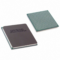
EP3C120F780C8 Altera, EP3C120F780C8 Datasheet - Page 65

EP3C120F780C8
Manufacturer Part Number
EP3C120F780C8
Description
IC CYCLONE III FPGA 119K 780FBGA
Manufacturer
Altera
Series
Cyclone® IIIr
Datasheets
1.EP3C5F256C8N.pdf
(5 pages)
2.EP3C5F256C8N.pdf
(34 pages)
3.EP3C5F256C8N.pdf
(66 pages)
4.EP3C5F256C8N.pdf
(14 pages)
5.EP3C5F256C8N.pdf
(76 pages)
Specifications of EP3C120F780C8
Number Of Logic Elements/cells
119088
Number Of Labs/clbs
7443
Total Ram Bits
3981312
Number Of I /o
531
Voltage - Supply
1.15 V ~ 1.25 V
Mounting Type
Surface Mount
Operating Temperature
0°C ~ 85°C
Package / Case
780-FBGA
For Use With
544-2601 - KIT DEV CYCLONE III LS EP3CLS200544-2589 - KIT DEV EMB CYCLONE III EDITION544-2566 - KIT DEV DSP CYCLONE III EDITION544-2444 - KIT DEV CYCLONE III EP3C120544-2411 - KIT DEV NIOS II CYCLONE III ED.
Lead Free Status / RoHS Status
Contains lead / RoHS non-compliant
Number Of Gates
-
Other names
544-2391
544-2531
544-2531
EP3C120F780C8ES
544-2531
544-2531
EP3C120F780C8ES
Available stocks
Company
Part Number
Manufacturer
Quantity
Price
Company:
Part Number:
EP3C120F780C8
Manufacturer:
ALTERA
Quantity:
561
Company:
Part Number:
EP3C120F780C8N
Manufacturer:
ALTERA
Quantity:
642
Part Number:
EP3C120F780C8N
Manufacturer:
ALTERA/阿尔特拉
Quantity:
20 000
Chapter 2: Cyclone III LS Device Data Sheet
Switching Characteristics
© December 2009
Altera Corporation
Table 2–30. Cyclone III LS Devices Emulated LVDS with Three-Resistor Network Transmitter Timing
Specifications
Table 2–31. Cyclone III LS Devices LVDS Receiver Timing Specifications
f
frequency)
HSIODR
t
TCCS
Output jitter
(peak to peak)
t
Notes to
(1) Emulated LVDS with three-resistor network transmitter is supported at the output pin of all I/O banks.
(2) t
(Part 1 of 2) (Preliminary)
f
frequency)
HSIODR
SW
HSC LK
DUTY
LOCK
HSC LK
(2)
LOC K
Symbol
Symbol
(input clock
(input clock
Table
is the time required for the PLL to lock from the end of device configuration.
2–30:
(Note 1)
Modes
Modes
(Preliminary)
×10
×10
×10
×10
×8
×7
×4
×2
×1
×8
×7
×4
×2
×1
—
×8
×7
×4
×2
×1
×8
×7
×4
×2
×1
—
—
—
—
Min
100
Min
100
10
10
10
10
10
10
80
70
40
20
10
—
10
10
10
10
10
10
80
70
40
20
10
45
—
—
—
C7 and I7
C7 and I7
402.5
402.5
402.5
402.5
Max
Max
370
370
370
370
370
740
740
740
740
740
400
320
320
320
320
320
640
640
640
640
640
200
500
55
1
Cyclone III Device Handbook, Volume 2
Min
100
Min
100
10
10
10
10
10
10
80
70
40
20
10
—
10
10
10
10
10
10
80
70
40
20
10
45
—
—
—
(Note 1)
C8
C8
402.5
402.5
402.5
402.5
Max
Max
320
320
320
320
320
640
640
640
640
640
400
275
275
275
275
275
550
550
550
550
550
200
550
55
1
Mbps
Mbps
Mbps
Mbps
Mbps
Mbps
Mbps
Mbps
Mbps
Mbps
Mbps
Mbps
MHz
MHz
MHz
MHz
MHz
MHz
Unit
Unit
MHz
MHz
MHz
MHz
MHz
MHz
ms
ps
ps
%
%
2–21


