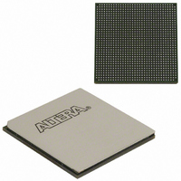
EP2SGX60EF1152I4 Altera, EP2SGX60EF1152I4 Datasheet - Page 104

EP2SGX60EF1152I4
Manufacturer Part Number
EP2SGX60EF1152I4
Description
IC STRATIX II GX 60K 1152-FBGA
Manufacturer
Altera
Series
Stratix® II GXr
Datasheet
1.EP2SGX30DF780C5.pdf
(316 pages)
Specifications of EP2SGX60EF1152I4
Number Of Logic Elements/cells
60440
Number Of Labs/clbs
3022
Total Ram Bits
2544192
Number Of I /o
534
Voltage - Supply
1.15 V ~ 1.25 V
Mounting Type
Surface Mount
Operating Temperature
-40°C ~ 100°C
Package / Case
1152-FBGA
Family Name
Stratix II GX
Number Of Logic Blocks/elements
60440
# I/os (max)
534
Frequency (max)
732.1MHz
Process Technology
SRAM
Operating Supply Voltage (typ)
1.2V
Logic Cells
60440
Ram Bits
2544192
Operating Supply Voltage (min)
1.15V
Operating Supply Voltage (max)
1.25V
Operating Temp Range
-40C to 100C
Operating Temperature Classification
Industrial
Mounting
Surface Mount
Pin Count
1152
Package Type
FC-FBGA
Lead Free Status / RoHS Status
Contains lead / RoHS non-compliant
Number Of Gates
-
Lead Free Status / Rohs Status
Not Compliant
Other names
544-2186
Available stocks
Company
Part Number
Manufacturer
Quantity
Price
Company:
Part Number:
EP2SGX60EF1152I4N
Manufacturer:
ALTERA
Quantity:
534
- Current page: 104 of 316
- Download datasheet (2Mb)
PLLs and Clock Networks
Figure 2–69. External PLL Output Clock Control Blocks
Notes to
(1)
(2)
2–96
Stratix II GX Device Handbook, Volume 1
These clock select signals can only be set through a configuration file (.sof or .pof) and cannot be dynamically
controlled during user mode operation.
The clock control block feeds to a multiplexer within the PLL_OUT pin’s IOE. The PLL_OUT pin is a dual-purpose
pin. Therefore, this multiplexer selects either an internal signal or the output of the clock control block.
Figure
2–69:
For the global clock control block, the clock source selection can be
controlled either statically or dynamically. You have the option of
statically selecting the clock source by using the Quartus II software to set
specific configuration bits in the configuration file (.sof
control the selection dynamically by using internal logic to drive the
multiplexer select inputs. When selecting statically, the clock source can
be set to any of the inputs to the select multiplexer. When selecting the
clock source dynamically, you can either select between two PLL outputs
(such as the C0 or C1 outputs from one PLL), between two PLLs (such as
the C0/C1 clock output of one PLL or the C0/C1 c1ock output of the other
PLL), between two clock pins (such as CLK0 or CLK1), or between a
combination of clock pins or PLL outputs.
For the regional and PLL_OUT clock control block, the clock source
selection can only be controlled statically using configuration bits. Any of
the inputs to the clock select multiplexer can be set as the clock source.
IOE
Internal
Logic
(2)
Outputs (c[5..0])
PLL Counter
PLL_OUT
Enable/
Disable
Pin
6
Internal
Static Clock
Select (1)
Logic
Static Clock Select
(1)
Altera Corporation
or .pof
October 2007
) or you can
Related parts for EP2SGX60EF1152I4
Image
Part Number
Description
Manufacturer
Datasheet
Request
R

Part Number:
Description:
4. Serial Configuration Devices Epcs1, Epcs4, Epcs16, Epcs64, And Epcs128 Data Sheet
Manufacturer:
Altera Corporation
Datasheet:

Part Number:
Description:
CYCLONE II STARTER KIT EP2C20N
Manufacturer:
Altera
Datasheet:

Part Number:
Description:
CPLD, EP610 Family, ECMOS Process, 300 Gates, 16 Macro Cells, 16 Reg., 16 User I/Os, 5V Supply, 35 Speed Grade, 24DIP
Manufacturer:
Altera Corporation
Datasheet:

Part Number:
Description:
CPLD, EP610 Family, ECMOS Process, 300 Gates, 16 Macro Cells, 16 Reg., 16 User I/Os, 5V Supply, 15 Speed Grade, 24DIP
Manufacturer:
Altera Corporation
Datasheet:

Part Number:
Description:
Manufacturer:
Altera Corporation
Datasheet:

Part Number:
Description:
CPLD, EP610 Family, ECMOS Process, 300 Gates, 16 Macro Cells, 16 Reg., 16 User I/Os, 5V Supply, 30 Speed Grade, 24DIP
Manufacturer:
Altera Corporation
Datasheet:

Part Number:
Description:
High-performance, low-power erasable programmable logic devices with 8 macrocells, 10ns
Manufacturer:
Altera Corporation
Datasheet:

Part Number:
Description:
High-performance, low-power erasable programmable logic devices with 8 macrocells, 7ns
Manufacturer:
Altera Corporation
Datasheet:

Part Number:
Description:
Classic EPLD
Manufacturer:
Altera Corporation
Datasheet:

Part Number:
Description:
High-performance, low-power erasable programmable logic devices with 8 macrocells, 10ns
Manufacturer:
Altera Corporation
Datasheet:

Part Number:
Description:
Manufacturer:
Altera Corporation
Datasheet:

Part Number:
Description:
Manufacturer:
Altera Corporation
Datasheet:

Part Number:
Description:
Manufacturer:
Altera Corporation
Datasheet:


