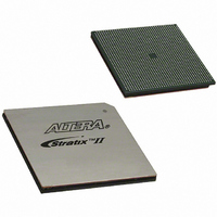
EP2S180F1508C3 Altera, EP2S180F1508C3 Datasheet - Page 11

EP2S180F1508C3
Manufacturer Part Number
EP2S180F1508C3
Description
IC STRATIX II FPGA 180K 1508FBGA
Manufacturer
Altera
Series
Stratix® IIr
Datasheet
1.EP2S15F484I4N.pdf
(238 pages)
Specifications of EP2S180F1508C3
Number Of Logic Elements/cells
179400
Number Of Labs/clbs
8970
Total Ram Bits
9383040
Number Of I /o
1170
Voltage - Supply
1.15 V ~ 1.25 V
Mounting Type
Surface Mount
Operating Temperature
0°C ~ 85°C
Package / Case
1508-FBGA
Family Name
Stratix II
Number Of Logic Blocks/elements
179400
# I/os (max)
1170
Frequency (max)
778.82MHz
Process Technology
90nm (CMOS)
Operating Supply Voltage (typ)
1.2V
Logic Cells
179400
Ram Bits
9383040
Operating Supply Voltage (min)
1.15V
Operating Supply Voltage (max)
1.25V
Operating Temp Range
0C to 85C
Operating Temperature Classification
Commercial
Mounting
Surface Mount
Pin Count
1508
Package Type
FC-FBGA
For Use With
544-1701 - DSP PRO KIT W/SII EP2S180N
Lead Free Status / RoHS Status
Contains lead / RoHS non-compliant
Number Of Gates
-
Lead Free Status / Rohs Status
Not Compliant
Other names
544-2164
Available stocks
Company
Part Number
Manufacturer
Quantity
Price
Company:
Part Number:
EP2S180F1508C3
Manufacturer:
ALTERA
Quantity:
3 000
Company:
Part Number:
EP2S180F1508C3N
Manufacturer:
ALTERA
Quantity:
624
Part Number:
EP2S180F1508C3N
Manufacturer:
ALTERA/阿尔特拉
Quantity:
20 000
Logic Array
Blocks
Altera Corporation
May 2007
EP2S15
EP2S30
EP2S60
EP2S90
EP2S130
EP2S180
Table 2–1. Stratix II Device Resources
Device
Columns/Blocks
M512 RAM
11 / 930
4 / 104
6 / 202
7 / 329
8 / 488
9 / 699
The number of M512 RAM, M4K RAM, and DSP blocks varies by device
along with row and column numbers and M-RAM blocks.
the resources available in Stratix II devices.
Each LAB consists of eight ALMs, carry chains, shared arithmetic chains,
LAB control signals, local interconnect, and register chain connection
lines. The local interconnect transfers signals between ALMs in the same
LAB. Register chain connections transfer the output of an ALM register to
the adjacent ALM register in an LAB. The Quartus
associated logic in an LAB or adjacent LABs, allowing the use of local,
shared arithmetic chain, and register chain connections for performance
and area efficiency.
Columns/Blocks
M4K RAM
4 / 144
5 / 255
6 / 408
7 / 609
8 / 768
3 / 78
Figure 2–2
M-RAM
Blocks
0
1
2
4
6
9
shows the Stratix II LAB structure.
Columns/Blocks
DSP Block
Stratix II Device Handbook, Volume 1
2 / 12
2 / 16
3 / 36
3 / 48
3 / 63
4 / 96
®
Columns
II Compiler places
Stratix II Architecture
LAB
100
30
49
62
71
81
Table 2–1
LAB Rows
26
36
51
68
87
96
lists
2–3


