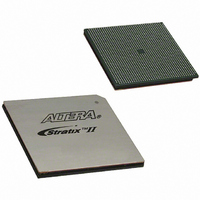
EP2S180F1508C3 Altera, EP2S180F1508C3 Datasheet - Page 203

EP2S180F1508C3
Manufacturer Part Number
EP2S180F1508C3
Description
IC STRATIX II FPGA 180K 1508FBGA
Manufacturer
Altera
Series
Stratix® IIr
Datasheet
1.EP2S15F484I4N.pdf
(238 pages)
Specifications of EP2S180F1508C3
Number Of Logic Elements/cells
179400
Number Of Labs/clbs
8970
Total Ram Bits
9383040
Number Of I /o
1170
Voltage - Supply
1.15 V ~ 1.25 V
Mounting Type
Surface Mount
Operating Temperature
0°C ~ 85°C
Package / Case
1508-FBGA
Family Name
Stratix II
Number Of Logic Blocks/elements
179400
# I/os (max)
1170
Frequency (max)
778.82MHz
Process Technology
90nm (CMOS)
Operating Supply Voltage (typ)
1.2V
Logic Cells
179400
Ram Bits
9383040
Operating Supply Voltage (min)
1.15V
Operating Supply Voltage (max)
1.25V
Operating Temp Range
0C to 85C
Operating Temperature Classification
Commercial
Mounting
Surface Mount
Pin Count
1508
Package Type
FC-FBGA
For Use With
544-1701 - DSP PRO KIT W/SII EP2S180N
Lead Free Status / RoHS Status
Contains lead / RoHS non-compliant
Number Of Gates
-
Lead Free Status / Rohs Status
Not Compliant
Other names
544-2164
Available stocks
Company
Part Number
Manufacturer
Quantity
Price
Company:
Part Number:
EP2S180F1508C3
Manufacturer:
ALTERA
Quantity:
3 000
Company:
Part Number:
EP2S180F1508C3N
Manufacturer:
ALTERA
Quantity:
624
Part Number:
EP2S180F1508C3N
Manufacturer:
ALTERA/阿尔特拉
Quantity:
20 000
Altera Corporation
April 2011
LVTTL
2.5-V LVTTL/CMOS
1.8-V LVTTL/CMOS
1.5-V LVTTL/CMOS
LVCMOS
SSTL-2 Class I
SSTL-2 Class II
SSTL-18 Class I
SSTL-18 Class II
1.5-V HSTL Class I
1.5-V HSTL Class II
1.8-V HSTL Class I
Table 5–77. Maximum Input Toggle Rate on Stratix II Devices (Part 1 of 2)
Input I/O Standard
The maximum clock toggle rate is different from the maximum data bit
rate. If the maximum clock toggle rate on a regular I/O pin is 300 MHz,
the maximum data bit rate for dual data rate (DDR) could be potentially
as high as 600 Mbps on the same I/O pin.
Table 5–77
specifies the maximum output clock toggle rates at 0pF load.
specifies the derating factors for the output clock toggle rate for a non 0pF
load.
To calculate the output toggle rate for a non 0pF load, use this formula:
The toggle rate for a non 0pF load
For example, the output toggle rate at 0pF load for SSTL-18 Class II 20mA
I/O standard is 550 MHz on a -3 device clock output pin. The derating
factor is 94ps/pF. For a 10pF load the toggle rate is calculated as:
Column I/O Pins (MHz)
500
500
500
500
500
500
500
500
500
500
500
500
-3
= 1000 / (1000/ toggle rate at 0pF load + derating factor * load value
in pF /1000)
Tables 5–77
devices.
1000 / (1000/550 + 94 × 10 /1000) = 363 (MHz)
500
500
500
500
500
500
500
500
500
500
500
500
-4
specifies the maximum input clock toggle rates.
through
450
450
450
450
450
500
500
500
500
500
500
500
-5
5–79
500
500
500
500
500
500
500
500
500
500
500
500
-3
Row I/O Pins (MHz)
show the I/O toggle rates for Stratix II
500
500
500
500
500
500
500
500
500
500
500
500
-4
Stratix II Device Handbook, Volume 1
450
450
450
450
450
500
500
500
500
500
500
500
-5
DC & Switching Characteristics
Dedicated Clock Inputs
500
500
500
500
500
500
500
500
500
500
500
500
-3
(MHz)
Table 5–78
500
500
500
500
500
500
500
500
500
500
500
500
-4
Table 5–79
400
400
400
400
400
500
500
500
500
500
500
500
-5
5–67


