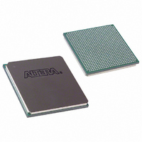
EP3C120F780C7N Altera, EP3C120F780C7N Datasheet - Page 57

EP3C120F780C7N
Manufacturer Part Number
EP3C120F780C7N
Description
IC CYCLONE III FPGA 119K 780FBGA
Manufacturer
Altera
Series
Cyclone® IIIr
Datasheets
1.EP3C5F256C8N.pdf
(5 pages)
2.EP3C5F256C8N.pdf
(34 pages)
3.EP3C5F256C8N.pdf
(66 pages)
4.EP3C5F256C8N.pdf
(14 pages)
5.EP3C5F256C8N.pdf
(76 pages)
6.EP3C120F780C7N.pdf
(274 pages)
Specifications of EP3C120F780C7N
Number Of Logic Elements/cells
119088
Number Of Labs/clbs
7443
Total Ram Bits
3981312
Number Of I /o
531
Voltage - Supply
1.15 V ~ 1.25 V
Mounting Type
Surface Mount
Operating Temperature
0°C ~ 85°C
Package / Case
780-FBGA
Family Name
Cyclone III
Number Of Logic Blocks/elements
119088
# I/os (max)
531
Frequency (max)
437.5MHz
Process Technology
65nm
Operating Supply Voltage (typ)
1.2V
Logic Cells
119088
Ram Bits
3981312
Operating Supply Voltage (min)
1.15V
Operating Supply Voltage (max)
1.25V
Operating Temp Range
0C to 85C
Operating Temperature Classification
Commercial
Mounting
Surface Mount
Pin Count
780
Package Type
FBGA
For Use With
544-2601 - KIT DEV CYCLONE III LS EP3CLS200544-2589 - KIT DEV EMB CYCLONE III EDITION544-2566 - KIT DEV DSP CYCLONE III EDITION544-2444 - KIT DEV CYCLONE III EP3C120544-2411 - KIT DEV NIOS II CYCLONE III ED.
Lead Free Status / RoHS Status
Lead free / RoHS Compliant
Number Of Gates
-
Lead Free Status / Rohs Status
Compliant
Other names
544-2394
544-2532
544-2532
EP3C120F780C7NES
544-2532
544-2532
EP3C120F780C7NES
Available stocks
Company
Part Number
Manufacturer
Quantity
Price
Company:
Part Number:
EP3C120F780C7N
Manufacturer:
SPANSION
Quantity:
1 000
Company:
Part Number:
EP3C120F780C7N
Manufacturer:
ALTERA
Quantity:
19
Chapter 2: Cyclone III LS Device Data Sheet
Electrical Characteristics
Table 2–18. Differential I/O Standard Specifications
Power Consumption
© December 2009
BLVDS
(Row
I/Os)
BLVDS
(Column
I/Os)
mini-LVDS
(Row
I/Os)
mini-LVDS
(Column
I/Os)
RSDS
(Row
I/Os)
RSDS
(Column
I/Os)
PPDS
(Row
I/Os)
PPDS
(Column
I/Os)
Notes to
(1) For an explanation of the terms used in
(2) R
(3) The LVPECL input standard is only supported at clock input. The output standard is not supported.
(4) There is no fixed V
(5) Mini-LVDS, RSDS, and PPDS standards are only supported at output pins of Cyclone III LS devices.
Standard
I/O
(4)
(4)
(5)
(5)
(5)
(5)
(5)
(5)
L
range: 90 ≤ R
Table
2.375
2.375
2.375
2.375
2.375
2.375
2.375
2.375
2–18:
Min
Altera Corporation
L
≤ 110 Ω.
V
ICM
C CIO
Typ
2.5
2.5
2.5
2.5
2.5
2.5
2.5
2.5
, V
Use the following methods to estimate power for your design:
■
■
Use the interactive Excel-based EPE before designing your device to get a magnitude
estimate of the device power. The Quartus II PowerPlay power analyzer provides
better quality estimates based on the specifics of the design after place-and-route is
complete. The PowerPlay power analyzer can apply a combination of user-entered,
simulation-derived, and estimated signal activities which, combined with detailed
circuit models, can yield very accurate power estimates.
(V)
OD
, and V
The Excel-based EPE
The Quartus II
2.625
2.625
2.625
2.625
2.625
2.625
2.625
2.625
Max
OS
specification for BLVDS. They are dependent on the system topology.
Min Max Min
100 —
100 —
—
—
—
—
—
—
V
Table
ID
(mV)
2–18, refer to
—
—
—
—
—
—
®
PowerPlay power analyzer feature
—
—
—
—
—
—
—
—
(Note 1)
“Transmitter Output Waveform”
Condition
(Part 2 of 2)
V
ICM
—
—
—
—
—
—
—
—
(V)
Max Min Typ Max
—
—
—
—
—
—
—
—
in
300
300
100 200
100 200
100 200
100 200
“Glossary” on page
—
—
V
O D
(mV)
—
—
—
—
Cyclone III Device Handbook, Volume 2
(2)
600
600
600
600
600
600
—
—
2–26.
Min
1.0
1.0
0.5
0.5
0.5
0.5
—
—
V
OS
Typ
(V)
1.2
1.2
1.2
1.2
1.2
1.2
—
—
(2)
Max
1.4
1.4
1.5
1.5
1.4
1.4
—
—
2–13


