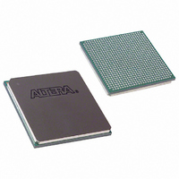
EP3C120F780C7N Altera, EP3C120F780C7N Datasheet - Page 74

EP3C120F780C7N
Manufacturer Part Number
EP3C120F780C7N
Description
IC CYCLONE III FPGA 119K 780FBGA
Manufacturer
Altera
Series
Cyclone® IIIr
Datasheets
1.EP3C5F256C8N.pdf
(5 pages)
2.EP3C5F256C8N.pdf
(34 pages)
3.EP3C5F256C8N.pdf
(66 pages)
4.EP3C5F256C8N.pdf
(14 pages)
5.EP3C5F256C8N.pdf
(76 pages)
6.EP3C120F780C7N.pdf
(274 pages)
Specifications of EP3C120F780C7N
Number Of Logic Elements/cells
119088
Number Of Labs/clbs
7443
Total Ram Bits
3981312
Number Of I /o
531
Voltage - Supply
1.15 V ~ 1.25 V
Mounting Type
Surface Mount
Operating Temperature
0°C ~ 85°C
Package / Case
780-FBGA
Family Name
Cyclone III
Number Of Logic Blocks/elements
119088
# I/os (max)
531
Frequency (max)
437.5MHz
Process Technology
65nm
Operating Supply Voltage (typ)
1.2V
Logic Cells
119088
Ram Bits
3981312
Operating Supply Voltage (min)
1.15V
Operating Supply Voltage (max)
1.25V
Operating Temp Range
0C to 85C
Operating Temperature Classification
Commercial
Mounting
Surface Mount
Pin Count
780
Package Type
FBGA
For Use With
544-2601 - KIT DEV CYCLONE III LS EP3CLS200544-2589 - KIT DEV EMB CYCLONE III EDITION544-2566 - KIT DEV DSP CYCLONE III EDITION544-2444 - KIT DEV CYCLONE III EP3C120544-2411 - KIT DEV NIOS II CYCLONE III ED.
Lead Free Status / RoHS Status
Lead free / RoHS Compliant
Number Of Gates
-
Lead Free Status / Rohs Status
Compliant
Other names
544-2394
544-2532
544-2532
EP3C120F780C7NES
544-2532
544-2532
EP3C120F780C7NES
Available stocks
Company
Part Number
Manufacturer
Quantity
Price
Company:
Part Number:
EP3C120F780C7N
Manufacturer:
SPANSION
Quantity:
1 000
Company:
Part Number:
EP3C120F780C7N
Manufacturer:
ALTERA
Quantity:
19
2–30
Table 2–39. Glossary (Part 5 of 5)
Cyclone III Device Handbook, Volume 2
Letter
W
V
X
Y
Z
V
V
V
V
V
V
V
V
V
V
V
V
V
V
V
V
V
V
V
V
V
V
V
V
V
C M( DC)
DIF( AC )
DIF( DC)
IC M
ID
IH
IH(A C)
IH(DC )
IL
IL ( AC )
IL ( DC)
IN
OC M
OD
OH
OL
OS
OX ( AC)
REF
REF (A C)
REF (DC )
S WING (A C)
S WING (DC )
TT
X ( AC)
Term
—
—
—
—
DC common mode input voltage.
AC differential Input Voltage—The minimum AC input differential voltage required for
switching.
DC differential Input Voltage—The minimum DC input differential voltage required for
switching.
Input Common Mode Voltage—The common mode of the differential signal at the receiver.
Input differential Voltage Swing—The difference in voltage between the positive and
complementary conductors of a differential transmission at the receiver.
Voltage Input High—The minimum positive voltage applied to the input that is accepted by
the device as a logic high.
High-level AC input voltage.
High-level DC input voltage.
Voltage Input Low—The maximum positive voltage applied to the input that is accepted by
the device as a logic low.
Low-level AC input voltage.
Low-level DC input voltage.
DC input voltage.
Output Common Mode Voltage—The common mode of the differential signal at the
transmitter.
Output differential Voltage Swing—The difference in voltage between the positive and
complementary conductors of a differential transmission at the transmitter. V
Voltage Output High—The maximum positive voltage from an output that the device
considers will be accepted as the minimum positive high level.
Voltage Output Low—The maximum positive voltage from an output that the device considers
will be accepted as the maximum positive low level.
Output offset voltage—V
AC differential Output cross point voltage—The voltage at which the differential output signals
must cross.
Reference voltage for the SSTL and HSTL I/O standards.
AC input reference voltage for the SSTL and HSTL I/O standards. V
peak-to-peak AC noise on V
DC input reference voltage for the SSTL and HSTL I/O standards.
AC differential Input Voltage—AC Input differential voltage required for switching. Refer to
Input Waveforms for the SSTL Differential I/O Standard.
DC differential Input Voltage—DC Input differential voltage required for switching. Refer to
Input Waveforms for the SSTL Differential I/O Standard.
Termination voltage for the SSTL and HSTL I/O standards.
AC differential Input cross point Voltage—The voltage at which the differential input signals
must cross.
OS
= (V
REF
must not exceed 2% of V
OH
+ V
OL
) / 2.
Definitions
—
—
—
—
REF (DC)
Chapter 2: Cyclone III LS Device Data Sheet
.
© December 2009 Altera Corporation
REF (AC )
= V
REF (DC)
OD
= V
+ noise. The
OH
– V
Glossary
OL
.


