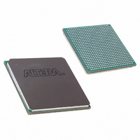
EP20K400EFC672-2X Altera, EP20K400EFC672-2X Datasheet - Page 52

EP20K400EFC672-2X
Manufacturer Part Number
EP20K400EFC672-2X
Description
IC APEX 20KE FPGA 400K 672-FBGA
Manufacturer
Altera
Series
APEX-20K®r
Datasheet
1.EP20K30ETC144-3.pdf
(117 pages)
Specifications of EP20K400EFC672-2X
Number Of Logic Elements/cells
16640
Number Of Labs/clbs
1664
Total Ram Bits
212992
Number Of I /o
488
Number Of Gates
1052000
Voltage - Supply
1.71 V ~ 1.89 V
Mounting Type
Surface Mount
Operating Temperature
0°C ~ 85°C
Package / Case
672-FBGA
Family Name
APEX 20K
Number Of Usable Gates
400000
Number Of Logic Blocks/elements
16640
# Registers
104
# I/os (max)
488
Frequency (max)
223MHz
Process Technology
SRAM
Operating Supply Voltage (typ)
1.8V
Logic Cells
16640
Ram Bits
212992
Device System Gates
1052000
Operating Supply Voltage (min)
1.71V
Operating Supply Voltage (max)
1.89V
Operating Temp Range
0C to 85C
Operating Temperature Classification
Commercial
Mounting
Surface Mount
Pin Count
672
Package Type
FC-FBGA
Lead Free Status / RoHS Status
Contains lead / RoHS non-compliant
Other names
544-2095
Available stocks
Company
Part Number
Manufacturer
Quantity
Price
Company:
Part Number:
EP20K400EFC672-2X
Manufacturer:
ALTERA
Quantity:
586
Part Number:
EP20K400EFC672-2X
Manufacturer:
ALTERA/阿尔特拉
Quantity:
20 000
Company:
Part Number:
EP20K400EFC672-2XB
Manufacturer:
ALTERA
Quantity:
3 000
APEX 20K Programmable Logic Device Family Data Sheet
52
Notes to
(1)
(2)
(3)
(4)
t
t
t
t
t
t
t
OUTJITTER
OUTDUTY
LOCK
Table 17. APEX 20KE ClockLock & ClockBoost Parameters
R
F
INDUTY
INJITTER
Symbol
To implement the ClockLock and ClockBoost circuitry with the Quartus II software, designers must specify the
input frequency. The Quartus II software tunes the PLL in the ClockLock and ClockBoost circuitry to this frequency.
The f
device operation. Simulation does not reflect this parameter.
Twenty-five thousand parts per million (PPM) equates to 2.5% of input clock period.
During device configuration, the ClockLock and ClockBoost circuitry is configured before the rest of the device. If
the incoming clock is supplied during configuration, the ClockLock and ClockBoost circuitry locks during
configuration because the t
The t
(2)
Table
,
CLKDEV
JITTER
(3)
16:
specification is measured under long-term observation.
Input rise time
Input fall time
Input duty cycle
Input jitter peak-to-peak
Jitter on ClockLock or ClockBoost-
generated clock
Duty cycle for ClockLock or
ClockBoost-generated clock
Time required for ClockLock or
ClockBoost to acquire lock
parameter specifies how much the incoming clock can differ from the specified frequency during
Parameter
Tables 17
for APEX 20KE devices.
LOCK
value is less than the time required for configuration.
and
18
summarize the ClockLock and ClockBoost parameters
Conditions
Note (1)
Min
40
45
Typ
output period
2% of input
Altera Corporation
0.35% of
period
Max
60
55
40
5
5
peak-to-
RMS
Unit
peak
µs
ns
ns
%
%


