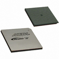
EP2SGX130GF1508I4N Altera, EP2SGX130GF1508I4N Datasheet - Page 311

EP2SGX130GF1508I4N
Manufacturer Part Number
EP2SGX130GF1508I4N
Description
IC STRATIX II GX 130K 1508-FBGA
Manufacturer
Altera
Series
Stratix® II GXr
Datasheet
1.EP2SGX30DF780C5.pdf
(316 pages)
Specifications of EP2SGX130GF1508I4N
Number Of Logic Elements/cells
132540
Number Of Labs/clbs
6627
Total Ram Bits
6747840
Number Of I /o
734
Voltage - Supply
1.15 V ~ 1.25 V
Mounting Type
Surface Mount
Operating Temperature
-40°C ~ 100°C
Package / Case
1508-FBGA
Family Name
Stratix II GX
Number Of Logic Blocks/elements
132540
# I/os (max)
734
Frequency (max)
732.1MHz
Process Technology
SRAM
Operating Supply Voltage (typ)
1.2V
Logic Cells
132540
Ram Bits
6747840
Operating Supply Voltage (min)
1.15V
Operating Supply Voltage (max)
1.25V
Operating Temp Range
-40C to 100C
Operating Temperature Classification
Industrial
Mounting
Surface Mount
Pin Count
1508
Package Type
FC-FBGA
Lead Free Status / RoHS Status
Lead free / RoHS Compliant
Number Of Gates
-
Lead Free Status / Rohs Status
Compliant
Other names
544-2175
Available stocks
Company
Part Number
Manufacturer
Quantity
Price
Company:
Part Number:
EP2SGX130GF1508I4N
Manufacturer:
Sunon
Quantity:
1 000
Part Number:
EP2SGX130GF1508I4N
Manufacturer:
ALTERA/阿尔特拉
Quantity:
20 000
- Current page: 311 of 316
- Download datasheet (2Mb)
April 2006, v3.0
February 2006,
v2.1
December 2005,
v2.0
October 2005
v1.1
October 2005
v1.0
Table 4–118. Document Revision History (Part 5 of 5)
Document
Date and
Version
●
●
●
●
●
●
●
●
●
●
●
Updated timing numbers.
●
●
●
●
Added chapter to the Stratix II GX Device
Handbook.
Updated Table 6–3.
Updated Table 6–5.
Updated Table 6–7.
Added Table 6–42.
Updated “Internal Timing Parameters” section
(Tables 6–43 through 6–48).
Updated “Stratix II GX Clock Timing
Parameters” section (Tables 6–49 through
6–65).
Updated “IOE Programmable Delay” section
(Tables 6–67 and 6–68)
Updated “I/O Delays” section (Tables 6–71
through 6–74.
Updated “Maximum Input & Output Clock Toggle
Rate” section. Replaced tables 6-73 and 6-74
with Tables 6–75 through 6–83. Input and output
clock rates for row, column, and dedicated clock
pins are now in separate tables.
Updated Tables 6–4 and 6–5.
Updated Tables 6–49 through 6–65 (removed
column designations for industrial/commercial
and removed industrial numbers).
Updated Table 6–7.
Updated Table 6–38.
Updated 3.3-V PCML information and notes to
Tables 6–73 through 6–76.
Minor textual changes throughout the
document.
Changes Made
Summary of Changes
Related parts for EP2SGX130GF1508I4N
Image
Part Number
Description
Manufacturer
Datasheet
Request
R

Part Number:
Description:
CYCLONE II STARTER KIT EP2C20N
Manufacturer:
Altera
Datasheet:

Part Number:
Description:
CPLD, EP610 Family, ECMOS Process, 300 Gates, 16 Macro Cells, 16 Reg., 16 User I/Os, 5V Supply, 35 Speed Grade, 24DIP
Manufacturer:
Altera Corporation
Datasheet:

Part Number:
Description:
CPLD, EP610 Family, ECMOS Process, 300 Gates, 16 Macro Cells, 16 Reg., 16 User I/Os, 5V Supply, 15 Speed Grade, 24DIP
Manufacturer:
Altera Corporation
Datasheet:

Part Number:
Description:
Manufacturer:
Altera Corporation
Datasheet:

Part Number:
Description:
CPLD, EP610 Family, ECMOS Process, 300 Gates, 16 Macro Cells, 16 Reg., 16 User I/Os, 5V Supply, 30 Speed Grade, 24DIP
Manufacturer:
Altera Corporation
Datasheet:

Part Number:
Description:
High-performance, low-power erasable programmable logic devices with 8 macrocells, 10ns
Manufacturer:
Altera Corporation
Datasheet:

Part Number:
Description:
High-performance, low-power erasable programmable logic devices with 8 macrocells, 7ns
Manufacturer:
Altera Corporation
Datasheet:

Part Number:
Description:
Classic EPLD
Manufacturer:
Altera Corporation
Datasheet:

Part Number:
Description:
High-performance, low-power erasable programmable logic devices with 8 macrocells, 10ns
Manufacturer:
Altera Corporation
Datasheet:

Part Number:
Description:
Manufacturer:
Altera Corporation
Datasheet:

Part Number:
Description:
Manufacturer:
Altera Corporation
Datasheet:

Part Number:
Description:
Manufacturer:
Altera Corporation
Datasheet:

Part Number:
Description:
CPLD, EP610 Family, ECMOS Process, 300 Gates, 16 Macro Cells, 16 Reg., 16 User I/Os, 5V Supply, 25 Speed Grade, 24DIP
Manufacturer:
Altera Corporation
Datasheet:


