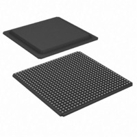
XC3SD1800A-4FGG676I Xilinx Inc, XC3SD1800A-4FGG676I Datasheet - Page 96

XC3SD1800A-4FGG676I
Manufacturer Part Number
XC3SD1800A-4FGG676I
Description
SPARTAN-3ADSP FPGA 1800K 676FBGA
Manufacturer
Xilinx Inc
Series
Spartan™-3A DSPr
Datasheets
1.XC3S50A-4VQG100C.pdf
(7 pages)
2.XC3SD3400A-4FGG676C.pdf
(4 pages)
3.XC3SD3400A-4FGG676C.pdf
(101 pages)
Specifications of XC3SD1800A-4FGG676I
Total Ram Bits
1548288
Number Of Logic Elements/cells
37440
Number Of Labs/clbs
4160
Number Of I /o
519
Number Of Gates
1800000
Voltage - Supply
1.14 V ~ 1.26 V
Mounting Type
Surface Mount
Operating Temperature
-40°C ~ 100°C
Package / Case
676-BBGA
No. Of Logic Blocks
4224
No. Of Gates
1800000
No. Of Macrocells
37440
Family Type
Spartan-3A
No. Of Speed Grades
4
No. Of I/o's
519
Clock
RoHS Compliant
Lead Free Status / RoHS Status
Lead free / RoHS Compliant
For Use With
122-1574 - KIT DEVELOPMENT SPARTAN 3ADSP
Lead Free Status / RoHS Status
Lead free / RoHS Compliant
Available stocks
Company
Part Number
Manufacturer
Quantity
Price
Company:
Part Number:
XC3SD1800A-4FGG676I
Manufacturer:
XILINX
Quantity:
591
Company:
Part Number:
XC3SD1800A-4FGG676I
Manufacturer:
Xilinx Inc
Quantity:
10 000
Company:
Part Number:
XC3SD1800A-4FGG676I
Manufacturer:
XILINX
Quantity:
160
User I/Os by Bank
Table 69
AWAKE pin is counted as a dual-purpose I/O.
Table 69: User I/Os Per Bank for the XC3SD3400A in the FG676 Package
DS610 (v3.0) October 4, 2010
Product Specification
Notes:
1.
Top
Right
Bottom
Left
Package
TOTAL
26 VREF are on INPUT pins.
Edge
indicates how the available user-I/O pins are distributed between the four I/O banks on the FG676 package. The
I/O Bank
0
1
2
3
Maximum I/Os
Input-Only
and
111
123
112
123
469
314
I/O
82
67
68
97
www.xilinx.com
INPUT
Spartan-3A DSP FPGA Family: Pinout Descriptions
11
34
8
6
9
All Possible I/O Pins by Type
DUAL
30
21
52
1
0
VREF
10
37
9
9
9
(1)
CLK
32
8
8
8
8
96


