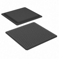
XCV405E-7FG676C Xilinx Inc, XCV405E-7FG676C Datasheet - Page 118

XCV405E-7FG676C
Manufacturer Part Number
XCV405E-7FG676C
Description
IC FPGA 1.8V C-TEMP 676-FBGA
Manufacturer
Xilinx Inc
Series
Virtex™-E EMr
Datasheet
1.XCV405E-6FG676C.pdf
(118 pages)
Specifications of XCV405E-7FG676C
Number Of Logic Elements/cells
10800
Number Of Labs/clbs
2400
Total Ram Bits
573440
Number Of I /o
404
Number Of Gates
129600
Voltage - Supply
1.71 V ~ 1.89 V
Mounting Type
Surface Mount
Operating Temperature
0°C ~ 85°C
Package / Case
676-BBGA
Lead Free Status / RoHS Status
Contains lead / RoHS non-compliant
Available stocks
Company
Part Number
Manufacturer
Quantity
Price
Company:
Part Number:
XCV405E-7FG676C
Manufacturer:
XilinxInc
Quantity:
3 000
Part Number:
XCV405E-7FG676C
Manufacturer:
XILINX/赛灵思
Quantity:
20 000
Virtex™-E 1.8 V Extended Memory Field Programmable Gate Arrays
Revision History
The following table shows the revision history for this document.
Virtex-E Extended Memory Data Sheet
The Virtex-E Extended Memory Data Sheet contains the following modules:
•
•
Module 4 of 4
42
03/23/00
08/01/00
09/19/00
11/20/00
04/02/01
07/23/01
07/17/02
Date
DS025-1, Virtex-E 1.8V Extended Memory FPGAs:
Introduction and Ordering Information (Module 1)
DS025-2, Virtex-E 1.8V Extended Memory FPGAs:
Functional Description (Module 2)
Version
1.0
1.1
1.2
1.3
1.4
1.5
1.6
•
•
•
•
•
•
•
•
•
•
•
•
Initial Xilinx release.
Accumulated edits and fixes. Upgrade to Preliminary. Preview -8 numbers added. Reformatted
to adhere to corporate documentation style guidelines. Minor changes in BG560 pin-out table.
In Table 3 (Module 4), FG676 Fine-Pitch BGA — XCV405E, the following pins are no longer
labeled as VREF: B7, G16, G26, W26, AF20, AF8, Y1, H1.
Min values added to Virtex-E Electrical Characteristics tables.
Updated speed grade -8 numbers in Virtex-E Electrical Characteristics tables (Module 3).
Updated minimums in Table 11 (Module 2), and added notes to Table 12 (Module 2).
Added to note 2 of Absolute Maximum Ratings (Module 3).
Changed all minimum hold times to –0.4 for Global Clock Set-Up and Hold for LVTTL
Standard, with DLL (Module 3).
Revised maximum T
In
pin G16 is now labeled as VREF.
Updated values in
Converted data sheet to modularized format. See the
Sheet
Changed definition of T31 and T32 pins in
Data sheet designation upgraded from Preliminary to Production.
Table
section.
4, FG676 Fine-Pitch BGA — XCV405E, pin B19 is no longer labeled as VREF, and
Virtex-E Switching Characteristics
DLLPW
www.xilinx.com
1-800-255-7778
in -6 speed grade for DLL Timing Parameters (Module 3).
•
•
DS025-3, Virtex-E 1.8V Extended Memory FPGAs:
DC and Switching Characteristics (Module 3)
DS025-4, Virtex-E 1.8V Extended Memory FPGAs:
Pinout Tables (Module 4)
Revision
Table 1
for XCV405E and the XCV812E devices.
tables.
Virtex-E Extended Memory Data
DS025-4 (v1.6) July 17, 2002
R


