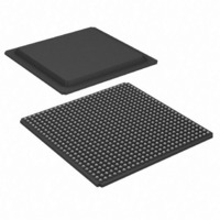
XCV405E-7FG676C Xilinx Inc, XCV405E-7FG676C Datasheet - Page 6

XCV405E-7FG676C
Manufacturer Part Number
XCV405E-7FG676C
Description
IC FPGA 1.8V C-TEMP 676-FBGA
Manufacturer
Xilinx Inc
Series
Virtex™-E EMr
Datasheet
1.XCV405E-6FG676C.pdf
(118 pages)
Specifications of XCV405E-7FG676C
Number Of Logic Elements/cells
10800
Number Of Labs/clbs
2400
Total Ram Bits
573440
Number Of I /o
404
Number Of Gates
129600
Voltage - Supply
1.71 V ~ 1.89 V
Mounting Type
Surface Mount
Operating Temperature
0°C ~ 85°C
Package / Case
676-BBGA
Lead Free Status / RoHS Status
Contains lead / RoHS non-compliant
Available stocks
Company
Part Number
Manufacturer
Quantity
Price
Company:
Part Number:
XCV405E-7FG676C
Manufacturer:
XilinxInc
Quantity:
3 000
Part Number:
XCV405E-7FG676C
Manufacturer:
XILINX/赛灵思
Quantity:
20 000
Virtex™-E 1.8 V Extended Memory Field Programmable Gate Arrays
Table 1:
In addition to the CLK and CE control signals, the three
flip-flops share a Set/Reset (SR). For each flip-flop, this sig-
nal can be independently configured as a synchronous Set,
a synchronous Reset, an asynchronous Preset, or an asyn-
chronous Clear.
The output buffer and all of the IOB control signals have
independent polarity controls.
All pads are protected against damage from electrostatic
discharge (ESD) and from over-voltage transients. After
configuration, clamping diodes are connected to V
the exception of LVCMOS18, LVCMOS25, GTL, GTL+,
LVDS, and LVPECL.
Optional pull-up, pull-down and weak-keeper circuits are
attached to each pad. Prior to configuration all outputs not
involved in configuration are forced into their high-imped-
ance state. The pull-down resistors and the weak-keeper
circuits are inactive, but IOs can optionally be pulled up.
The activation of pull-up resistors prior to configuration is
controlled on a global basis by the configuration mode pins.
If the pull-up resistors are not activated, all the pins are in a
high-impedance state. Consequently, external pull-up or
pull-down resistors must be provided on pins required to be
at a well-defined logic level prior to configuration.
Module 2 of 4
2
BLVDS & LVDS
HSTL III & IV
SSTL3 I & II
SSTL2 I & II
LVCMOS18
LVCMOS2
Standard
PCI33_3
PCI66_3
AGP-2X
LVPECL
HSTL I
LVTTL
GTL+
GTL
CTT
I/O
Supported I/O Standards
Output
V
N/A
N/A
3.3
2.5
1.8
3.3
2.5
1.5
1.5
3.3
3.3
3.3
3.3
2.5
3.3
CCO
Input
V
N/A
N/A
N/A
N/A
N/A
N/A
N/A
N/A
N/A
N/A
3.3
2.5
1.8
3.3
3.3
CCO
Input
V
1.50
1.25
0.80
0.75
0.90
1.50
1.32
N/A
N/A
N/A
N/A
N/A
N/A
N/A
1.0
REF
Termination
Voltage
Board
(V
1.50
1.25
1.20
1.50
0.75
1.50
1.50
N/A
N/A
N/A
N/A
N/A
N/A
N/A
N/A
CCO
TT
)
www.xilinx.com
1-800-255-7778
with
All Virtex-E IOBs support IEEE 1149.1-compatible bound-
ary scan testing.
Input Path
The Virtex-E IOB input path routes the input signal directly
to internal logic and/ or through an optional input flip-flop.
An optional delay element at the D-input of this flip-flop elim-
inates pad-to-pad hold time. The delay is matched to the
internal clock-distribution delay of the FPGA, and when
used, assures that the pad-to-pad hold time is zero.
Each input buffer can be configured to conform to any of the
low-voltage signalling standards supported. In some of
these standards the input buffer utilizes a user-supplied
threshold voltage, V
constraints on which standards can be used in close prox-
imity to each other.
There are optional pull-up and pull-down resistors at each
user I/O input for use after configuration. Their value is in
the range 50 - 100 kΩ.
Output Path
The output path includes a 3-state output buffer that drives
the output signal onto the pad. The output signal can be
routed to the buffer directly from the internal logic or through
an optional IOB output flip-flop.
The 3-state control of the output can also be routed directly
from the internal logic or through a flip-flip that provides syn-
chronous enable and disable.
Each output driver can be individually programmed for a
wide range of low-voltage signalling standards. Each output
buffer can source up to 24 mA and sink up to 48 mA. Drive
strength and slew rate controls minimize bus transients.
In most signalling standards, the output High voltage
depends on an externally supplied V
to supply V
can be used in close proximity to each other.
ing" on page 2.
An optional weak-keeper circuit is connected to each out-
put. When selected, the circuit monitors the voltage on the
pad and weakly drives the pin High or Low to match the
input signal. If the pin is connected to a multiple-source sig-
nal, the weak keeper holds the signal in its last state if all
drivers are disabled. Maintaining a valid logic level in this
way eliminates bus chatter.
Since the weak-keeper circuit uses the IOB input buffer to
monitor the input level, an appropriate V
provided if the signalling standard requires one. The provi-
sion of this voltage must comply with the I/O banking rules.
I/O Banking
Some of the I/O standards described above require V
and/or V
plied and connected to device pins that serve groups of
REF
CCO
voltages. These voltages are externally sup-
imposes constraints on which standards
See "I/O Banking" on page 2.
REF
. The need to supply V
DS025-2 (v2.3) November 19, 2002
CCO
REF
voltage. The need
voltage must be
See "I/O Bank-
REF
imposes
CCO
R


