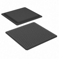
XCV405E-7FG676C Xilinx Inc, XCV405E-7FG676C Datasheet - Page 53

XCV405E-7FG676C
Manufacturer Part Number
XCV405E-7FG676C
Description
IC FPGA 1.8V C-TEMP 676-FBGA
Manufacturer
Xilinx Inc
Series
Virtex™-E EMr
Datasheet
1.XCV405E-6FG676C.pdf
(118 pages)
Specifications of XCV405E-7FG676C
Number Of Logic Elements/cells
10800
Number Of Labs/clbs
2400
Total Ram Bits
573440
Number Of I /o
404
Number Of Gates
129600
Voltage - Supply
1.71 V ~ 1.89 V
Mounting Type
Surface Mount
Operating Temperature
0°C ~ 85°C
Package / Case
676-BBGA
Lead Free Status / RoHS Status
Contains lead / RoHS non-compliant
Available stocks
Company
Part Number
Manufacturer
Quantity
Price
Company:
Part Number:
XCV405E-7FG676C
Manufacturer:
XilinxInc
Quantity:
3 000
Part Number:
XCV405E-7FG676C
Manufacturer:
XILINX/赛灵思
Quantity:
20 000
Creating LVDS Output 3-State Buffers
LVDS output 3-state buffers can be placed in a wide number
of IOB locations. The exact locations are dependent on the
package used. The Virtex-E package information lists the
possible locations as IO_L#P for the P-side and IO_L#N for
the N-side, where # is the pair number.
HDL Instantiation
Both output 3-state buffers are required to be instantiated in
the design and placed on the correct IO_L#P and IO_L#N
locations. The IOB must have the same net source the fol-
lowing pins, clock (C), set/reset (SR), 3-state (T), 3-state
clock enable (TCE), output (O), output clock enable (OCE).
In addition, the output (O) pins must be inverted with
respect to each other, and if output registers are used, the
INIT states must be opposite values (one High and one
Low). If 3-state registers are used, they must be initialized to
the same state. Failure to follow these rules leads to DRC
errors in the software.
VHDL Instantiation
Verilog Instantiation
Location Constraints
All LVDS buffers must be explicitly placed on a device. For
the output buffers this can be done with the following con-
straint in the UCF or NCF file.
Synchronous vs. Asynchronous 3-State Outputs
If the outputs are synchronous (registered in the IOB), then
any IO_L#P|N pair can be used. If the outputs are asynchro-
nous (no output register), then they must use one of the
pairs that are part of the same IOB group at the end of a
ROW or at the top/bottom of a COLUMN in the device. This
applies for either the 3-state pin or the data out pin.
DS025-2 (v2.3) November 19, 2002
data0_p:
(I=>data_int(0), T=>data_tri,
O=>data_p(0));
data0_inv: INV port map
(I=>data_int(0), O=>data_n_int(0));
data0_n:
(I=>data_n_int(0), T=>data_tri,
O=>data_n(0));
OBUFT_LVDS data0_p
.T(data_tri), .O(data_p[0]));
INV
.O(data_n_int[0]);
OBUFT_LVDS data0_n
.T(data_tri), .O(data_n[0]));
NET data_p<0> LOC = D28; # IO_L0P
NET data_n<0> LOC = B29; # IO_L0N
R
data0_inv (.I(data_int[0],
OBUFT_LVDS port map
OBUFT_LVDS port map
(.I(data_n_int[0]),
(.I(data_int[0]),
Virtex™-E 1.8 V Extended Memory Field Programmable Gate Arrays
www.xilinx.com
1-800-255-7778
LVDS pairs that can be used as asynchronous outputs are
listed in the Virtex-E pinout tables. Some pairs are marked
as “asynchronous capable” for all devices in that package,
and others are marked as available only for that device in
the package. If the device size might be changed at some
point in the product lifetime, then only the common pairs for
all packages should be used.
Adding Output and 3-State Registers
All LVDS buffers can have an output register in the IOB. The
output registers must be in both the P-side and N-side IOBs.
All the normal IOB register options are available (FD, FDE,
FDC, FDCE, FDP, FDPE, FDR, FDRE, FDS, FDSE, LD,
LDE, LDC, LDCE, LDP, LDPE). The register elements can
be inferred or explicitly instantiated in the HDL code.
Special care must be taken to insure that the D pins of the
registers are inverted and that the INIT states of the regis-
ters are opposite. The 3-state (T), 3-state clock enable
(CE), clock pin (C), output clock enable (CE) and set/reset
(CLR/PRE or S/R) pins must connect to the same source.
Failure to do this leads to a DRC error in the software.
The register elements can be packed in the IOB using the
IOB property to TRUE on the register or by using the “map
-pr [i|o|b]” where “i” is inputs only, “o” is outputs only and “b”
is both inputs and outputs.
To improve design coding times VHDL and Verilog synthe-
sis macro libraries have been developed to explicitly create
these structures. The input library macros are listed below.
The 3-state is configured to be 3-stated at GSR and when
the PRE,CLR,S or R is asserted and shares it's clock
enable with the output register. If this is not desirable, the
library can be updated by the user for the desired function-
ality. The O and OB inputs to the macros are the external
net connections.
Creating LVDS Bidirectional Buffer
LVDS bidirectional buffers can be placed in a wide number
of IOB locations. The exact locations are dependent on the
package used. The Virtex-E package information lists the
possible locations as IO_L#P for the P-side and IO_L#N for
the N-side, where # is the pair number.
HDL Instantiation
Both bidirectional buffers are required to be instantiated in
the design and placed on the correct IO_L#P and IO_L#N
locations. The IOB must have the same net source the fol-
lowing pins, clock (C), set/reset (SR), 3-state (T), 3-state
clock enable (TCE), output (O), output clock enable (OCE).
In addition, the output (O) pins must be inverted with
respect to each other, and if output registers are used, the
INIT states must be opposite values (one HIGH and one
LOW). If 3-state registers are used, they must be initialized
to the same state. Failure to follow these rules leads to DRC
errors in the software.
Module 2 of 4
49


