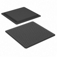
XCV405E-7FG676C Xilinx Inc, XCV405E-7FG676C Datasheet - Page 61

XCV405E-7FG676C
Manufacturer Part Number
XCV405E-7FG676C
Description
IC FPGA 1.8V C-TEMP 676-FBGA
Manufacturer
Xilinx Inc
Series
Virtex™-E EMr
Datasheet
1.XCV405E-6FG676C.pdf
(118 pages)
Specifications of XCV405E-7FG676C
Number Of Logic Elements/cells
10800
Number Of Labs/clbs
2400
Total Ram Bits
573440
Number Of I /o
404
Number Of Gates
129600
Voltage - Supply
1.71 V ~ 1.89 V
Mounting Type
Surface Mount
Operating Temperature
0°C ~ 85°C
Package / Case
676-BBGA
Lead Free Status / RoHS Status
Contains lead / RoHS non-compliant
Available stocks
Company
Part Number
Manufacturer
Quantity
Price
Company:
Part Number:
XCV405E-7FG676C
Manufacturer:
XilinxInc
Quantity:
3 000
Part Number:
XCV405E-7FG676C
Manufacturer:
XILINX/赛灵思
Quantity:
20 000
Virtex-E Switching Characteristics
All devices are 100% functionally tested. Internal timing parameters are derived from measuring internal test patterns. Listed
below are representative values. For more specific, more precise, and worst-case guaranteed data, use the values reported
by the static timing analyzer (TRCE in the Xilinx Development System) and back-annotated to the simulation net list. All
timing parameters assume worst-case operating conditions (supply voltage and junction temperature). Values apply to all
Virtex-E devices unless otherwise noted.
IOB Input Switching Characteristics
Input delays associated with the pad are specified for LVTTL levels. For other standards, adjust the delays with the values
shown in
DS025-3 (v2.3.2) March 14, 2003
Notes:
1.
2.
Propagation Delays
Pad to I output, no delay
Pad to I output, with delay
Pad to output IQ via transparent latch,
no delay
Pad to output IQ via transparent latch,
with delay
Propagation Delays
Clock
Minimum Pulse Width, High
Minimum Pulse Width, Low
Clock CLK to output IQ
Setup and Hold Times with respect to Clock at IOB Input Register
Pad, no delay
Pad, with delay
ICE input
SR input (IFF, synchronous)
Set/Reset Delays
SR input to IQ (asynchronous)
GSR to output IQ
A Zero “0” Hold Time listing indicates no hold time or a negative hold time. Negative values can not be guaranteed “best-case”, but
if a “0” is listed, there is no positive hold time.
Input timing i for LVTTL is measured at 1.4 V. For other I/O standards, see
‘‘IOB Input Switching Characteristics Standard Adjustments’’ on page
R
Description
(1)
T
T
T
T
T
T
Symbol
T
T
T
T
IOPICKD
IOICECK
T
T
T
IOPICK
IOICKPD
IOCKICE
IOSRCKI
T
IOCKIQ
IOSRIQ
IOPLID
IOICKP
T
GSRQ
T
IOPID
IOPLI
IOPI
CH
CL
Virtex™-E 1.8 V Extended Memory Field Programmable Gate Arrays
/
/
/
www.xilinx.com
1-800-255-7778
XCV405E
XCV812E
XCV405E
XCV812E
XCV405E
XCV812E
Device
All
All
All
All
All
All
All
All
0.69 / 0
1.49 / 0
1.49 / 0
0.28 /
Table
0.43
0.51
0.55
0.75
1.55
1.55
0.56
0.56
0.18
0.38
0.54
3.88
Min
0.0
3.
6.
1.3 / 0
3.4 / 0
3.4 / 0
0.55 /
Speed Grade
0.01
0.8
1.0
1.1
1.4
3.5
3.5
1.2
1.2
0.4
0.8
1.1
7.6
-8
1.4 / 0
3.5 / 0
3.5 / 0
0.7 /
0.01
0.8
1.0
1.1
1.5
3.6
3.6
1.3
1.3
0.7
0.9
1.2
8.5
-7
(2)
1.5 / 0
3.5 / 0
3.5 / 0
0.7 /
0.01
0.8
1.0
1.1
1.6
3.7
3.7
1.4
1.4
0.7
1.0
1.4
9.7
-6
Module 3 of 4
ns, max
ns, max
ns, max
ns, max
ns, max
ns, max
ns, max
ns, max
ns, max
ns, min
ns, min
ns, min
ns, min
ns, min
ns, min
ns, min
Units
5


