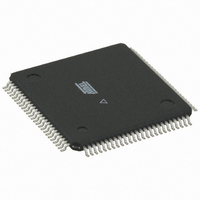
AT94K05AL-25AQU Atmel, AT94K05AL-25AQU Datasheet - Page 29

AT94K05AL-25AQU
Manufacturer Part Number
AT94K05AL-25AQU
Description
IC FPSLIC 5K GATE 25MHZ 100-TQFP
Manufacturer
Atmel
Series
FPSLIC®r
Datasheet
1.AT94K05AL-25AJI.pdf
(204 pages)
Specifications of AT94K05AL-25AQU
Core Type
8-bit AVR
Speed
25MHz
Interface
I²C, UART
Program Sram Bytes
4K-16K
Fpga Sram
2kb
Data Sram Bytes
4K ~ 16K
Fpga Core Cells
256
Fpga Gates
5K
Fpga Registers
436
Voltage - Supply
3 V ~ 3.6 V
Mounting Type
Surface Mount
Operating Temperature
-40°C ~ 85°C
Package / Case
100-TQFP, 100-VQFP
For Use With
ATSTK594 - BOARD FPSLIC DAUGHTER FOR STK500
Lead Free Status / RoHS Status
Lead free / RoHS Compliant
Eeprom Size
-
Available stocks
Company
Part Number
Manufacturer
Quantity
Price
- Current page: 29 of 204
- Download datasheet (4Mb)
3.5
3.6
1138I–FPSLI–1/08
AVR Cache Mode
Resets
The AVR has the ability to cache download the FPGA memory. The AVR has direct access to
the data buses of the FPGA’s configuration SRAM and is able to download bitstreams. AVR
Cache access of configuration SRAM is not available during normal configuration downloads.
The Cache Logic port in the AVR is located in the I/O memory map. Three registers, FPGAX,
FPGAY FPGAZ, control the address written to inside the FPGA; and FPGAD in the AVR mem-
ory map controls the Data. Registers FPGAX, FPGAY and FPGAZ are write only, see
Figure
Figure 3-6.
The AVR Cache Logic access mode is write only. Transfers may be aborted at any time due to
AVR program wishes or external interrupts.
The FPGA CHECK function is not supported by the AVR Cache mode.
A typical application for this mode is for the AVR to accept serial data through a UART for exam-
ple, and port it as configuration data to the FPGA, thereby affecting a download, or allowing
reconfigurable systems where the FPGA is updated algorithmically by the AVR. For more infor-
mation, refer to the “AT94K Series Configuration” application note available on the Atmel web
site, at: http://www.atmel.com/atmel/acrobat/doc2313.pdf.
The user must have the flexibility to issue resets and reconfiguration commands to separate por-
tions of the device. There are two Reset pins on the FPSLIC device. The first, RESET, results in
a clearing of all FPGA configuration SRAM and the System Control Register, and initiates a
download if in mode 0. The AVR will stop and be reset.
A second reset pin, AVRReset, is implemented to reset the AVR portion of the FPSLIC func-
tional blocks. This is described in the
interrupted during
(Operation is not
3-6.
FPGA CORE
EMBEDDED
Cache Logic
loading)
Internal FPGA Configuration Access
Configuration Clock – Each tick is generated when the Memory-
mapped I/O location FPGAD is written to inside the AVR.
24-bit Address Write
Memory Write Data
8-bit Configuration
CACHEIOWE
Configuration Logic
“Reset Sources” on page
AT94KAL Series FPSLIC
FPGAZ [7:0]
FPGAD [7:0]
FPGAX [7:0]
FPGAY [7:0]
63.
Memory-mapped
Memory-mapped
Memory-mapped
Memory-mapped
EMBEDDED
Location
Location
Location
Location
AVR CORE
29
Related parts for AT94K05AL-25AQU
Image
Part Number
Description
Manufacturer
Datasheet
Request
R

Part Number:
Description:
IC FPSLIC 5K GATE 25MHZ 84PLCC
Manufacturer:
Atmel
Datasheet:

Part Number:
Description:
Fpslic Devices Combine 5K Gates of Atmel's Patented AT40K Fpga Architecture, a 20 Mips Avr 8-bit Risc Microprocessor Core, Numerous Fixed Microcontroller Peripheries And up to 36K Bytes of Program And Data SRAM.
Manufacturer:
ATMEL Corporation
Datasheet:

Part Number:
Description:
IC FPSLIC 5K GATE 25MHZ 84PLCC
Manufacturer:
Atmel
Datasheet:

Part Number:
Description:
IC FPSLIC 5K GATE 25MHZ 208PQFP
Manufacturer:
Atmel
Datasheet:

Part Number:
Description:
IC FPSLIC 5K GATE 25MHZ 144LQFP
Manufacturer:
Atmel
Datasheet:

Part Number:
Description:
IC FPSLIC 5K GATE 25MHZ 208PQFP
Manufacturer:
Atmel
Datasheet:

Part Number:
Description:
IC FPSLIC 5K GATE 25MHZ 144LQFP
Manufacturer:
Atmel
Datasheet:

Part Number:
Description:
IC FPSLIC 5K GATE 25MHZ 144-LQFP
Manufacturer:
Atmel
Datasheet:

Part Number:
Description:
Manufacturer:
Atmel
Datasheet:

Part Number:
Description:
Manufacturer:
Atmel
Datasheet:

Part Number:
Description:
Manufacturer:
Atmel
Datasheet:

Part Number:
Description:
5k - 40k Gates Of At40k Fpga With 8-bit Microcontroller, Up To 36k Bytes Of Sram And On-chip Jtag Ice
Manufacturer:
ATMEL Corporation
Datasheet:

Part Number:
Description:
At94k05al 5k - 40k Gates Of At40k Fpga With 8-bit Microcontroller, Up To 36k Bytes Of Sram And On-chip Jtag Ice
Manufacturer:
ATMEL Corporation
Datasheet:

Part Number:
Description:
DEV KIT FOR AVR/AVR32
Manufacturer:
Atmel
Datasheet:


