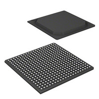
KSZ8692PBI Micrel Inc, KSZ8692PBI Datasheet - Page 22

KSZ8692PBI
Manufacturer Part Number
KSZ8692PBI
Description
IC ARM9 PHY 10/100MBPS 400-PBGA
Manufacturer
Micrel Inc
Datasheet
1.KSZ8692PBI.pdf
(42 pages)
Specifications of KSZ8692PBI
Applications
Networking & Communications
Core Processor
ARM9
Program Memory Type
External Program Memory
Controller Series
KSZ
Interface
EBI/EMI, Ethernet, I²C, I²S,PCI, SPI, UART/USART, USB
Number Of I /o
20
Voltage - Supply
1.235 V ~ 1.365 V
Operating Temperature
-40°C ~ 85°C
Mounting Type
Surface Mount
Package / Case
400-BGA
Operating Temp Range
-40C to 85C
Operating Temperature Classification
Industrial
Package Type
BGA
Mounting
Surface Mount
Lead Free Status / RoHS Status
Lead free / RoHS Compliant
Ram Size
-
Lead Free Status / RoHS Status
Supplier Unconfirmed, Lead free / RoHS Compliant
Other names
576-3627
KSZ8692PBI
KSZ8692PBI
Signal Descriptions by Group
Micrel, Inc.
March 2010
Pin Number
System Interface
NAND/SRAM/ROM/EXIO Interface
G3, G4, G2,
H2, G5, H1,
N4, P3, R2,
T1, M4, K5,
N3, P2, R1,
L4, M3, P1,
J3, H5, H4,
F1, G1, F2,
L2, K1, K2,
F3, F5, F4,
T2, U1, L5,
J2, H3, J1,
E1, E2, E3
W15, W14
W17, W16
Y15, Y14
Y17, Y16
T7, U7
H19
U13
W1
W3
R5
N5
Y1
Y3
K4
Pin Name
DDCLKON[1:0]
DDCLKON[3:2]
SADDR[23..0]
DDCLKO[1:0]
DDCLKO[3:2]
SDATA[15..0]
CLK25MHz
SDCLKEO
SDOCLK
RESETN
WRSTO
SDICLK
XCLK2
XCLK1
VREF
Pin Type
Ipu/O
O
O
O
O
O
O
O
O
O
I
I
I
I
I
Pin Description
Reset, asserted Low.
RESETN will force the KSZ8692PB to reset ARM9 CPU and all functional
blocks. Once asserted, RESETN must remain asserted for a minimum duration
of 256 system clock cycles. When in the reset state, all the output pins are put
into Tri-state and all open drain signals are floated.
Watchdog Timer Reset Output
When the Watchdog Timer expires, this signal will be asserted for at least 200
msec.
System Clock Input 2.
External crystal or clock input 2. The clock frequency should be 25MHz ±
100ppm.
System Clock Input 1.
Used with XCLK1 pin when other polarity of crystal is needed. This is unused
for a normal clock input.
25MHz output to external PHY
DDR Clock Out [1:0].
Output of the internal system clock, it is also used as the clock signal for DDR
interface.
The negative of differential pair of DDR Clock Out [1:0].
Output of the internal system clock, it is also used as the clock signal for DDR
interface.
Clock Enable output for SDRAM (for Power Down Mode)
Reference Voltage for SSTL interface.
Must be half of the voltage for the DDR VDD supply. See EIA/JEDEC standard
EIA/JESD8-9 (Stub series terminated logic for 2.5V, SSTL_2)
DDR Clock Out for loopback from De-skew PLL
DDR Clock In from loopback to De-skew PLL. This pin must connect to
SDOCLK with appropriate de-skew length. See Engineering Evaluation Design
Kit for detailed implementation.
Factory Reserved
Factory Reserved
SRAM Address Bus.
The 24-bit address bus covers 16M word memory space of
ROM/SRAM/FLASH, and 16M byte external I/O banks.
This address bus is shared between ROM/SRAM/FLASH/EXTIO devices.
SRAM DATA Bus.
Bidirectional Bus for 16-bit DATA In and DATA Out. The KSZ8692PB also
supports 8-bit data bus for ROM/SRAM/FLASH/EXTIO cycles.
This data bus is shared between NAND, ROM/SRAM/FLASH/EXTIO devices.
22
M9999-031810-4.0
KSZ8692PB


