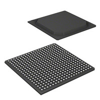
KSZ8692PBI Micrel Inc, KSZ8692PBI Datasheet - Page 8

KSZ8692PBI
Manufacturer Part Number
KSZ8692PBI
Description
IC ARM9 PHY 10/100MBPS 400-PBGA
Manufacturer
Micrel Inc
Datasheet
1.KSZ8692PBI.pdf
(42 pages)
Specifications of KSZ8692PBI
Applications
Networking & Communications
Core Processor
ARM9
Program Memory Type
External Program Memory
Controller Series
KSZ
Interface
EBI/EMI, Ethernet, I²C, I²S,PCI, SPI, UART/USART, USB
Number Of I /o
20
Voltage - Supply
1.235 V ~ 1.365 V
Operating Temperature
-40°C ~ 85°C
Mounting Type
Surface Mount
Package / Case
400-BGA
Operating Temp Range
-40C to 85C
Operating Temperature Classification
Industrial
Package Type
BGA
Mounting
Surface Mount
Lead Free Status / RoHS Status
Lead free / RoHS Compliant
Ram Size
-
Lead Free Status / RoHS Status
Supplier Unconfirmed, Lead free / RoHS Compliant
Other names
576-3627
KSZ8692PBI
KSZ8692PBI
ARM High-Performance Processor
The KSZ8692PB is built around the 16/32-bit ARM922T RISC processor designed by Advanced RISC Machines. The
ARM922T is a scalable, high-performance processor that was developed for highly integrated SoC applications. Its
simple, elegant, and fully static design is particularly suitable for cost-effective and power-sensitive embedded systems. It
also offers a separate 8KB D-cache and 8KB I-cache that reduces memory access latency.16-bit thumb instruction sets
are supported to minimize memory footprint. The ARM processor core can be programmed to maximum of 250 MHz for
highest possible performance.
The Advanced Microprocessor Bus Architecture/Advanced High-Performance Bus (AMBA AHB) is a 32-bit wide ARM
system bus to which is connected the processor, the register ports of the DDR memory controller, the
FLASH/ROM/SRAM/External I/O controller, the NAND memory controller, the Ethernet MACs, the PCI bridge, the USB
ports and the SDIO controller. The ARM processor is the master of AHB and responsible for configuring the operational
characteristics of each AHB device via their individual register port. The AHB is programmable up to 166MHz for
maximum system bus performance. AHB interfaces to devices are shown in functional block diagram.
Also connected to AHB is ARM Advanced Peripheral Bus or APB bridge which is attached the standard peripherals. The
APB Bridge transparently converts the AHB accesses into slower APB accesses. The ARM processor is the master of
APB bridge and responsible for configuring the operational characteristics and transfer of data for each APB attached
peripheral. APB interfaces to standard peripherals are shown in functional block diagram.
FLASH/ROM/SRAM Memory and External I/O Interface
The KSZ8692PB memory controller provides glueless interface for static memory, i.e. ROM, SRAM, and NOR Flash and
three banks of external I/O. NOR Flash bank0 can be configured by power-up strap option to operate as boot bank from a
8 or 16 bit device.
The memory interface for the static memory has a special automatic address mapping feature. This allows the designer to
connect address bit 0 on the memory to ADDR[0] on the KSZ8692PB and address bit 1 on the memory to ADDR[1] on the
KSZ8692PB, regardless of whether the designer is trying to achieve half word or byte addressing. The KSZ8692PB
memory controller performs the address mapping internally. This gives the designer the flexibilty to use 8 or 16 bit data
width devices interchangeably on the same PCB (see Figure 4). For external I/O, however, the designer still needs to
resolve the address mapping (see Figure 5).
Micrel, Inc.
March 2010
• 250MHz ARM922T RISC processor core
• 166MHz AMBA Bus 2.0
• 16-bit thumb instruction sets
• 8KB D-cache and 8KB I-cache
• Supports Little-Endian mode
• Configurable MMU
• Power saving options include clock down of both processor core and AMBA AHB
• Glueless connection to two banks of FLASH/ROM/SRAM memory with programmable 8 or 16 bit data width and
• Support for AMD/Intel like Flash
• Automatic address line mapping for 8 or 16-bit accesses on Flash, ROM, and SRAM interfaces
• Supports three external I/O banks with programmable 8 or 16 bit data width and programmable access timing
• Total 64MB address space for two banks of FLASH/ROM/SRAM and and three banks of external I/O
programmable access timing
8
M9999-031810-4.0
KSZ8692PB


