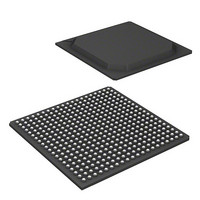
KSZ8692PBI Micrel Inc, KSZ8692PBI Datasheet - Page 35

KSZ8692PBI
Manufacturer Part Number
KSZ8692PBI
Description
IC ARM9 PHY 10/100MBPS 400-PBGA
Manufacturer
Micrel Inc
Datasheet
1.KSZ8692PBI.pdf
(42 pages)
Specifications of KSZ8692PBI
Applications
Networking & Communications
Core Processor
ARM9
Program Memory Type
External Program Memory
Controller Series
KSZ
Interface
EBI/EMI, Ethernet, I²C, I²S,PCI, SPI, UART/USART, USB
Number Of I /o
20
Voltage - Supply
1.235 V ~ 1.365 V
Operating Temperature
-40°C ~ 85°C
Mounting Type
Surface Mount
Package / Case
400-BGA
Operating Temp Range
-40C to 85C
Operating Temperature Classification
Industrial
Package Type
BGA
Mounting
Surface Mount
Lead Free Status / RoHS Status
Lead free / RoHS Compliant
Ram Size
-
Lead Free Status / RoHS Status
Supplier Unconfirmed, Lead free / RoHS Compliant
Other names
576-3627
KSZ8692PBI
KSZ8692PBI
Micrel, Inc.
March 2010
Pin Number
M1
R3
U2
J4
(WRSTPLS)
Pin Name
ERWEN0
EROEN
NCLE
NALE
Pin Type
Ipd/O
Ipd/O
Ipd/O
Ipd/O
Pin Description
ROM/SRAM/FLASH(NOR) and EXTIO Output Enable, asserted Low.
When asserted, this signal controls the output enable port of the specified
ROM/SRAM/FLASH memory and EXTIO device.
During reset, this pin is used for Watchdog Timer Reset Polarity Select.
This is a power strapping option pin for watchdog reset output polarity.
“0” = WRSTO is selected as active high (default)
“1” = WRSTO is selected as active low.
This pin is shared with the EROEN pin.
ROM/SRAM/FLASH(NOR) and EXTIO Write Byte Enable, asserted Low.
When asserted, these signals control the byte write enable of the memory device
for ROM/SRAM/FLASH and EXTIO access.
During ARM tic test mode, this pin is TESTACK.
During reset, this pin is input strap option to enable MII mode at port0 (WAN port)
0: MII mode (default)
1: Factory Reserved
NAND command Latch Enable
NCLE controls the activating path for command sent to NAND flash.
During reset, this pin is input strap option for NAND Flash configuration register
(0x8054) bit [2]. This bit along with configuration register bits [1:0] is used for boot
program. This pin along with NALE and NWEN is used to specify NAND Flash
size.
[NCLE, NALE, NWEN]
000 = 64Mbit
001 = 128Mbit (default)
010 = 256Mbit
011 = 512Mbit
100 = 1Gbit
101 = 2Gbit
110 = 4Gbit
111 = 8Gbit
NAND Address Latch Enable
NALE controls the activating path for address sent to NAND flash.
During reset, this pin is input strap option for NAND Flash configuration register
(0x8054) bit [1]. This bit along with configuration register bits [2], [0] is used for
boot program. This pin along with NCLE and NWEN is used to specify NAND
Flash size.
[NCLE, NALE, NWEN]
000 = 64Mbit
001 = 128Mbit (default)
010 = 256Mbit
011 = 512Mbit
100 = 1Gbit
101 = 2Gbit
110 = 4Gbit
111 = 8Gbit
35
M9999-031810-4.0
KSZ8692PB


