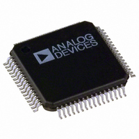
ADE7166ASTZF8 Analog Devices Inc, ADE7166ASTZF8 Datasheet - Page 105

ADE7166ASTZF8
Manufacturer Part Number
ADE7166ASTZF8
Description
IC ENERGY METER 1PHASE 64LQFP
Manufacturer
Analog Devices Inc
Specifications of ADE7166ASTZF8
Applications
Energy Measurement
Core Processor
8052
Program Memory Type
FLASH (8 kB)
Controller Series
ADE71xx
Ram Size
512 x 8
Interface
I²C, SPI, UART
Number Of I /o
20
Voltage - Supply
3.135 V ~ 3.465 V
Operating Temperature
-40°C ~ 85°C
Mounting Type
Surface Mount
Package / Case
64-LQFP
Ic Function
Single Phase Energy Measurement IC
Supply Voltage Range
3.13V To 3.46V, 2.4V To 3.7V
Operating Temperature Range
-40°C To +85°C
Digital Ic Case Style
LQFP
No. Of Pins
64
Lead Free Status / RoHS Status
Lead free / RoHS Compliant
Available stocks
Company
Part Number
Manufacturer
Quantity
Price
Company:
Part Number:
ADE7166ASTZF8
Manufacturer:
Analog Devices Inc
Quantity:
10 000
Company:
Part Number:
ADE7166ASTZF8-RL
Manufacturer:
Analog Devices Inc
Quantity:
10 000
Table 99. LCD Data Memory Accessed Indirectly Through LCD Pointer SFR (LCDPTR, Address 0xAC) and LCD Data SFR (LCDDAT,
Address 0xAE)
LCD Memory Address
0x0E
0x0D
0x0C
0x0B
0x0A
0x09
0x08
0x07
0x06
0x05
0x04
0x03
0x02
0x01
0x00
1
2
VOLTAGE GENERATION
The ADE7166/ADE7169/ADE7566/ADE7569 provide two ways
to generate the LCD waveform voltage levels. The on-chip charge
pump option can generate 5 V. This makes it possible to use 5 V
LCDs with the 3.3 V ADE7166/ADE7169/ADE7566/ADE7569.
There is also an option to use an external resistor ladder with a
3.3 V LCD. The EXTRES bit (Bit 6) in the LCD Configuration X
SFR (LCDCONX, Address 0x9C) selects the resistor ladder or
charge pump option. In the ADE7116 only, the resistor driver
option is available.
When selecting how to generate the LCD waveform voltages,
the following should be considered:
•
•
Lifetime Performance Power Consumption
In most LCDs, a high amount of current is required when the LCD
waveforms change state. The external resistor ladder option draws a
constant amount of current, whereas the charge pump circuitry
allows dynamic current consumption. If the LCD module is used
with the internal charge pump option when the display is disabled,
the voltage generation is disabled so that no power is consumed by
the LCD function. This feature results in significant power
savings if the display is turned off during battery operation.
COMx designates the common lines.
FPx designates the segment lines.
Lifetime performance power consumption
Contrast control
1, 2
COM3
FP27
FP25
FP23
FP21
FP19
FP17
FP15
FP13
FP11
FP9
FP7
FP5
FP3
FP1
LCD Pointer SFR (LCDPTR, Address 0xAC)
COM2
FP27
FP25
FP23
FP21
FP19
FP17
FP15
FP13
FP11
FP9
FP7
FP5
FP3
FP1
ADE7116/ADE7156/ADE7166/ADE7169/ADE7566/ADE7569
COM1
FP27
FP25
FP23
FP21
FP19
FP17
FP15
FP13
FP11
FP9
FP7
FP5
FP3
FP1
Rev. B | Page 105 of 152
COM0
FP27
FP25
FP23
FP21
FP19
FP17
FP15
FP13
FP11
FP9
FP7
FP5
FP3
FP1
Contrast Control
The electrical characteristics of the liquid in the LCD change
over temperature. This requires adjustments in the LCD waveform
voltages to ensure a readable display. An added benefit of the
internal charge pump voltage generation is a configurable bias
voltage that can be compensated over temperature and supply
to maintain contrast on the LCD. These compensations can be
performed based on the ADE7166/ADE7169/ADE7566/
ADE7569 temperature and supply voltage measurements (see
the Temperature, Battery, and Supply Voltage Measurements
section). This dynamic contrast control is not easily implemented
with external resistor ladder voltage generation.
The LCD bias voltage sets the contrast of the display when
the charge pump provides the LCD waveform voltages. The
ADE7166/ADE7169/ADE7566/ADE7569 provide 64 bias levels
selected by the BIASLVL[5:0] bits in the LCD Configuration X
SFR (LCDCONX, Address 0x9C). The voltage level on LCDVA,
LCDVB, and LCDVC depend on the internal voltage reference
value (VREF), BIASLVL[5:0] selection, and the biasing selected
as described in Table 90.
Lifetime Performance
DC offset on a segment degrades its performance over time.
The voltages generated through the internal charge pump
switch faster than those generated by the external resistor
ladder, reducing the likelihood of a dc voltage being applied
to a segment and increasing the lifetime of the LCD.
COM3
FP28
FP26
FP24
FP22
FP20
FP18
FP16
FP14
FP12
FP10
FP8
FP6
FP4
FP2
FP0
LCD Pointer SFR (LCDDAT, Address 0xAE)
COM2
FP28
FP26
FP24
FP22
FP20
FP18
FP16
FP14
FP12
FP10
FP8
FP6
FP4
FP2
FP0
COM1
FP28
FP26
FP24
FP22
FP20
FP18
FP16
FP14
FP12
FP10
FP8
FP6
FP4
FP2
FP0
COM0
FP28
FP26
FP24
FP22
FP20
FP18
FP16
FP14
FP12
FP10
FP8
FP6
FP4
FP2
FP0


