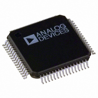
ADE7166ASTZF8 Analog Devices Inc, ADE7166ASTZF8 Datasheet - Page 114

ADE7166ASTZF8
Manufacturer Part Number
ADE7166ASTZF8
Description
IC ENERGY METER 1PHASE 64LQFP
Manufacturer
Analog Devices Inc
Specifications of ADE7166ASTZF8
Applications
Energy Measurement
Core Processor
8052
Program Memory Type
FLASH (8 kB)
Controller Series
ADE71xx
Ram Size
512 x 8
Interface
I²C, SPI, UART
Number Of I /o
20
Voltage - Supply
3.135 V ~ 3.465 V
Operating Temperature
-40°C ~ 85°C
Mounting Type
Surface Mount
Package / Case
64-LQFP
Ic Function
Single Phase Energy Measurement IC
Supply Voltage Range
3.13V To 3.46V, 2.4V To 3.7V
Operating Temperature Range
-40°C To +85°C
Digital Ic Case Style
LQFP
No. Of Pins
64
Lead Free Status / RoHS Status
Lead free / RoHS Compliant
Available stocks
Company
Part Number
Manufacturer
Quantity
Price
Company:
Part Number:
ADE7166ASTZF8
Manufacturer:
Analog Devices Inc
Quantity:
10 000
Company:
Part Number:
ADE7166ASTZF8-RL
Manufacturer:
Analog Devices Inc
Quantity:
10 000
ADE7116/ADE7156/ADE7166/ADE7169/ADE7566/ADE7569
Enabling Flash Protection by Emulator Commands
Another way to set the flash protection bytes is to use the
reserved emulator commands available only in download mode.
These commands write directly to the SFRs and can be used to
duplicate the operation described in the Enabling Flash
Protection by Code section. When these flash bytes are written,
the part can exit emulation mode by reset and the protections
are effective. This method can be used in production and
implemented after downloading the program. The commands
used for this operation are an extension of the commands listed
in Application Note uC004, Understanding the Serial Download
Protocol , available at www.analog.com.
•
•
Omitting the protocol defined in uC004, the sequence to load
protections is similar to the sequence mentioned in the
Enabling Flash Protection by Code section, except that two
emulator commands are necessary to replace one assembly
command. For example, to write the protection value in
EADRH (Address 0xC7), the following two commands must be
executed:
•
•
With this protocol, the protection can be written to the flash
memory using the same sequence as described in the Enabling
Flash Protection by Code section. When the part is reset, the
protection is effective.
Notes on Flash Protection
The flash protection scheme is disabled by default so that none
of the pages of the flash are protected from reading or writing/
erasing.
The last page must be write/erase protected for the protection
scheme to work.
To activate the protection settings, the ADE7116/ADE7156/
ADE7166/ADE7169/ADE7566/ADE7569 must be reset after
configuring the protection.
After configuring protection on the last page and resetting the
part, protections that have been enabled can be removed only
by mass erasing the flash memory. The protection bits are read
and erase protected by enabling read and write/erase protection
on the last page, but the protection bits are never truly write
protected.
Command with ASCII Code I or 0x49 writes the data into R0.
Command with ASCII Code F or 0x46 writes R0 into the
SFR address defined in the data of this command.
Command I with data = value of Protection Byte 0x3FFF.
Command F with data = 0xC7.
Rev. B | Page 114 of 152
Protection bits can be modified from a 1 to a 0, even after the
last page has been protected. In this way, more protection can
be added but none can be removed.
When the last page is read protected, the protection bits can still
be read by the user code. All other bits on this page are not
available for reading.
The protection scheme is intended to protect the end system. Pro-
tection should be disabled while developing and emulating code.
Flash Memory Timing
Typical program and erase times for the flash memory are
shown in Table 111.
Table 111. Flash Memory Program and Erase Times
Command
Write Byte
Erase Page
Erase All
Read Byte
Erase Page and Write Byte
Verify Byte
Note that the core microcontroller operation is idled until the
requested flash memory operation is complete. In practice, this
means that even though the flash operation is typically initiated
with a two-machine-cycle MOV instruction to write to the flash
control SFR (ECON, Address 0xB9), the next instruction is not
executed until the Flash/EE operation is complete. This means
that the core cannot respond to interrupt requests until the
Flash/EE operation is complete, although the core peripheral
functions, such as counter/timers, continue to count, as
configured throughout this period.
IN-CIRCUIT PROGRAMMING
Serial Downloading
The ADE7116/ADE7156/ADE7166/ADE7169/ADE7566/
ADE7569 facilitate code download via the standard UART
serial port. The parts enter serial download mode after a reset or
a power cycle if the SDEN pin is pulled low through an external
1 kΩ resistor. Once in serial download mode, the hidden
embedded download kernel executes. This allows the user to
download code to the full 16 kB of flash memory while the
device is in-circuit in its target application hardware.
Protection configured in the last page of the ADE7116/ADE7156/
ADE7166/ADE7169/ADE7566/ADE7569 affects whether flash
memory can be accessed in serial download mode. Read
protected pages cannot be read. Write/erase protected pages
cannot be written or erased.
Bytes
Affected
1 byte
512 bytes
16 kB
1 byte
512 bytes
1 byte
Flash Memory
Timing
30 μs
20 ms
200 ms
100 ns
21 ms
100 ns


