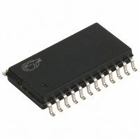
CY7C63613-SC Cypress Semiconductor Corp, CY7C63613-SC Datasheet - Page 18

CY7C63613-SC
Manufacturer Part Number
CY7C63613-SC
Description
IC MCU 8K USB LS MCU 24-SOIC
Manufacturer
Cypress Semiconductor Corp
Series
M8™r
Datasheet
1.CY7C63613-SC.pdf
(30 pages)
Specifications of CY7C63613-SC
Applications
USB Microcontroller
Core Processor
M8B
Program Memory Type
OTP (8 kB)
Controller Series
CY7C636xx
Ram Size
256 x 8
Interface
PS2, USB
Number Of I /o
16
Voltage - Supply
4 V ~ 5.5 V
Operating Temperature
0°C ~ 70°C
Mounting Type
Surface Mount
Package / Case
24-SOIC (7.5mm Width)
Lead Free Status / RoHS Status
Contains lead / RoHS non-compliant
Other names
428-1321
Available stocks
Company
Part Number
Manufacturer
Quantity
Price
Company:
Part Number:
CY7C63613-SC
Manufacturer:
CYP
Quantity:
5 510
Part Number:
CY7C63613-SC
Manufacturer:
CYPRESS/赛普拉斯
Quantity:
20 000
10.1
The enumeration sequence is shown below:
10.The USB Controller retrieves the descriptors from its program space and returns the data to the host over the USB.
10.2
PS/2 operation is possible with the CY7C636xx series through the use of firmware and several operating modes. The first enabling
feature:
Bits 5 and 4 of the Upstream Status and Control register are directly connected to the D+ and D USB pins of the CY7C636xx.
These pins constantly monitor the levels of these signals with CMOS input thresholds. Firmware can poll and decode these signal s
as PS/2 clock and data.
Bits [2:0] defaults to ‘000’ at reset which allows the USB SIE to control output on D+ and D . Firmware can override the SIE and
directly control the state of these pins via these 3 control bits. Since PS/2 is an open drain signaling protocol, these modes allow
all 4 PS/2 states to be generated on the D+ and D pins
10.3
USB status and control is regulated by the USB Status and Control Register located at I/O address 0x1Fh as shown in Figure
10-1 . This is a read/write register. All reserved bits must be written to zero. All bits in the register are cleared during reset.
The Bus Activity bit is a “sticky” bit that indicates if any non-idle USB event has occurred on the USB bus. The user firmware
should check and clear this bit periodically to detect any loss of bus activity. Writing a “0” to the Bus Activity bit clears it while
writing a “1” preserves the current value. In other words, the firmware can clear the Bus Activity bit, but only the SIE can set it.
The 1.024-ms timer interrupt service routine is normally used to check and clear the Bus Activity bit. The following table shows
how the control bits are encoded for this register.
1. The host computer sends a Setup packet followed by a Data packet to USB address 0 requesting the Device descriptor.
2. The USB Controller decodes the request and retrieves its Device descriptor from the program memory space.
3. The host computer performs a control read sequence and the USB Controller responds by sending the Device descriptor over
4. After receiving the descriptor, the host computer sends a Setup packet followed by a Data packet to address 0 assigning a
5. The USB Controller stores the new address in its USB Device Address Register after the no-data control sequence is complete.
6. The host sends a request for the Device descriptor using the new USB address.
7. The USB Controller decodes the request and retrieves the Device descriptor from the program memory.
8. The host performs a control read sequence and the USB Controller responds by sending its Device descriptor over the USB bus.
9. The host generates control reads to the USB Controller to request the Configuration and Report descriptors.
1. USB Bus reset on D+ and D is an interrupt that can be disabled;
2. USB traffic can be disabled via bit 7 of the USB register;
3. D+ and D can be monitored and driven via firmware as independent port bits.
the USB bus.
new USB address to the device.
Reserved
7
USB Enumeration
PS/2 Operation
USB Port Status and Control
Reserved
6
Figure 10-1. USB Status and Control Register 0x1Fh
D+
FOR
R
5
PRELIMINARY
D–
R
4
18
Bus Activity
R/W
3
Control
Bit 2
R/W
2
Control
Bit 1
R/W
1
CY7C63612/13
Control
R/W
Bit 0
0


