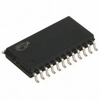
CY7C63613-SC Cypress Semiconductor Corp, CY7C63613-SC Datasheet - Page 20

CY7C63613-SC
Manufacturer Part Number
CY7C63613-SC
Description
IC MCU 8K USB LS MCU 24-SOIC
Manufacturer
Cypress Semiconductor Corp
Series
M8™r
Datasheet
1.CY7C63613-SC.pdf
(30 pages)
Specifications of CY7C63613-SC
Applications
USB Microcontroller
Core Processor
M8B
Program Memory Type
OTP (8 kB)
Controller Series
CY7C636xx
Ram Size
256 x 8
Interface
PS2, USB
Number Of I /o
16
Voltage - Supply
4 V ~ 5.5 V
Operating Temperature
0°C ~ 70°C
Mounting Type
Surface Mount
Package / Case
24-SOIC (7.5mm Width)
Lead Free Status / RoHS Status
Contains lead / RoHS non-compliant
Other names
428-1321
Available stocks
Company
Part Number
Manufacturer
Quantity
Price
Company:
Part Number:
CY7C63613-SC
Manufacturer:
CYP
Quantity:
5 510
Part Number:
CY7C63613-SC
Manufacturer:
CYPRESS/赛普拉斯
Quantity:
20 000
The ‘set-up’ PID status (bit[7]) is forced HIGH from the start of the data packet phase of the set-up transaction, until the start of
the ACK packet returned by the SIE. The CPU is prevented from clearing this bit during this interval, and subsequently until the
CPU first does an IORD to this endpoint 0 mode register.
Bits[6:0] of the endpoint 0 mode register are locked from CPU IOWR operations only if the SIE has updated one of these bits,
which the SIE does only at the end of a packet transaction (set-up ... Data ... ACK, or Out ... Data ... ACK, or In ... Data ... ACK).
The CPU can unlock these bits by doing a subsequent I/O read of this register.
Firmware must do an IORD after an IOWR to an endpoint 0 register to verify that the contents have changed and that the SIE
has not updated these values.
While the ‘set-up’ bit is set, the CPU cannot write to the DMA buffers at memory locations 0xE0 through 0xE7 and 0xF8 through
0xFF. This prevents an incoming set-up transaction from conflicting with a previous In data buffer filling operation by firmware.
The mode bits (bits [3:0]) in an Endpoint Mode Register control how the endpoint responds to USB bus traffic. The mode bit
encoding is shown in Section 15.0.
The format of the endpoint Device counter registers is shown below:
Bits 0 to 3 indicate the number of data bytes to be transmitted during an IN packet, valid values are 0 to 8 inclusive. Data Valid
bit 6 is used for OUT and set-up tokens only. Data 0/1 Toggle bit 7 selects the DATA packet’s toggle state: 0 for DATA0, 1 for DATA1.
12.0
The 12-bit timer provides two interrupts (128- s and 1.024-ms) and allows the firmware to directly time events that are up to 4
ms in duration. The lower 8 bits of the timer can be read directly by the firmware. Reading the lower 8 bits latches the upper 4
bits into a temporary register. When the firmware reads the upper 4 bits of the timer, it is actually reading the count stored in the
temporary register. The effect of this logic is to ensure a stable 12-bit timer value can be read, even when the two reads are
separated in time.
12.1
12.2
Reserved
Data 0/1
Toggle
Timer
Bit 7
Timer (LSB)
Timer (MSB)
12-bit Free-running Timer
11
L3
D3
Data Valid
Reserved
Timer
10
L2
Bit 6
Figure 11-4. USB Device Counter Registers 0x11h, 0x13h, 0x15h (read/write)
D2
9
L1
D1
8
L0
Reserved
Reserved
D0
Timer
Bit 5
FOR
Figure 12-1. Timer Register 0x24h (read only)
Figure 12-2. Timer Register 0x25h (read only)
7
PRELIMINARY
D7
Figure 12-3. Timer Block Diagram
6
D6
Reserved
Reserved
5
Timer
Bit 4
D5
4
D4
20
3
Byte count
D3
Timer
Timer
Bit 11
Bit 3
Bit 3
2
D2
1
D1
Byte count
8
0
Timer
Timer
Bit 10
Bit 2
Bit 2
D0
1.024-ms interrupt
128- s interrupt
1-MHz clock
To Timer Register
Byte count
Timer
Timer
Bit 1
Bit 1
Bit 9
CY7C63612/13
Byte count
Timer
Timer
Bit 0
Bit 0
Bit 8


