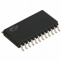
CY7C63613-SC Cypress Semiconductor Corp, CY7C63613-SC Datasheet - Page 28

CY7C63613-SC
Manufacturer Part Number
CY7C63613-SC
Description
IC MCU 8K USB LS MCU 24-SOIC
Manufacturer
Cypress Semiconductor Corp
Series
M8™r
Datasheet
1.CY7C63613-SC.pdf
(30 pages)
Specifications of CY7C63613-SC
Applications
USB Microcontroller
Core Processor
M8B
Program Memory Type
OTP (8 kB)
Controller Series
CY7C636xx
Ram Size
256 x 8
Interface
PS2, USB
Number Of I /o
16
Voltage - Supply
4 V ~ 5.5 V
Operating Temperature
0°C ~ 70°C
Mounting Type
Surface Mount
Package / Case
24-SOIC (7.5mm Width)
Lead Free Status / RoHS Status
Contains lead / RoHS non-compliant
Other names
428-1321
Available stocks
Company
Part Number
Manufacturer
Quantity
Price
Company:
Part Number:
CY7C63613-SC
Manufacturer:
CYP
Quantity:
5 510
Part Number:
CY7C63613-SC
Manufacturer:
CYPRESS/赛普拉斯
Quantity:
20 000
18.0
Notes:
.
10. Total current cumulative across all Port pins flowing to V
11. Irange: Isinkn(15)/ Isinkn(0) for the same pin.
12. Measured at crossover point of differential data signals.
13. Tested at 200 pF.
14. Limits total bus capacitance loading (C
15. DAC I/O Port not bonded out on CY7C63612/13. See note on page 16 for firmware code needed for unused pins.
Parameter
t
t
t
t
t
t
t
t
V
t
t
t
t
t
t
t
t
t
3.
4.
5.
6.
7.
8.
9.
CYC
CH
CL
r
r
f
f
rfm
drate
djr1
djr2
deop
eopr1
eopr2
eopt
udj1
udj2
crs
Functionality is guaranteed of the V
USB transmitter functionality is guaranteed over the V
Per Table 7-7 of revision 1.1 of USB specification, for C
Port 3 bit 7 controls whether the parts goes into suspend after a POR event or waits 128 ms to begin running.
POR will re-occur whenever V
Measured as largest step size vs. nominal according to measured full scale and zero programmed values.
T
ratio
= Isink1[1:0](n)/Isink0[7:2](n) for the same n, programmed.
Switching Characteristics
Input Clock Cycle Time
Clock HIGH Time
Clock LOW Time
Transition Rise Time
Transition Rise Time
Transition Fall Time
Transition Fall Time
Rise/Fall Time Matching
Output Signal Crossover Voltage
Low Speed Data Rate
Receiver Data Jitter Tolerance
Receiver Data Jitter Tolerance
Differential to EOP Transition Skew
EOP Width at Receiver
EOP Width at Receiver
Source EOP Width
Differential Driver Jitter
Differential Driver Jitter
USB Driver Characteristics
USB Data Timing
Description
Clock
CC
drops to approximately 2.5V.
CLOCK
CC (1)
LOAD
range, except USB transmitter and DACs.
) to 400 pF per section 7.1.5 of revision 1.1 of USB specification.
FOR
PRELIMINARY
CC (2)
LOAD
SS
0.45 t
0.45 t
Figure 18-1. Clock Timing
is limited to minimize Ground-Drop noise effects.
range, as well as DAC outputs.
1.4775
of 50–600 pF.
165.0
–150
Min.
1.25
–75
–45
–40
330
675
–95
1.3
75
75
80
CYC
CYC
t
CH
28
1.5225
t
168.3
Max.
CYC
1.50
300
300
125
100
150
2.0
75
45
95
t
CL
Unit
Mbs
ns
ns
ns
ns
ns
ns
ns
ns
ns
ns
ns
ns
ns
ns
%
V
s
CLoad = 50 pF (notes 4,5)
CLoad = 600 pF (notes 4,5)
CLoad = 50 pF (notes 4,5)
CLoad = 600 pF (notes 4,5)
t
Ave. Bit Rate (1.5Mb/s ± 1.5%)
To Next Transition (note 12)
For Paired Transitions (note 12)
(note 10)
Rejects as EOP (note 12)
Accepts as EOP (note 12)
To next transition, Figure 18-5
To paired transition, Figure 18-5
r
/t
f
(note 13)
Conditions
CY7C63612/13


