MPC8248VRPIEA Freescale Semiconductor, MPC8248VRPIEA Datasheet - Page 19
MPC8248VRPIEA
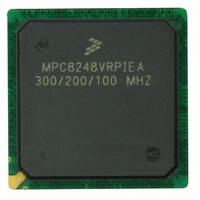
Manufacturer Part Number
MPC8248VRPIEA
Description
IC MPU POWERQUICC II 516-PBGA
Manufacturer
Freescale Semiconductor
Series
PowerQUICC IIr
Datasheet
1.MPC8248VRMIBA.pdf
(60 pages)
Specifications of MPC8248VRPIEA
Processor Type
MPC82xx PowerQUICC II 32-bit
Speed
300MHz
Voltage
1.5V
Mounting Type
Surface Mount
Package / Case
516-PBGA
Processor Series
MPC8xxx
Core
603e
Data Bus Width
32 bit
Maximum Clock Frequency
300 MHz
Operating Supply Voltage
1.4 V to 1.6 V
Maximum Operating Temperature
+ 105 C
Mounting Style
SMD/SMT
Data Ram Size
4 KB
Minimum Operating Temperature
0 C
Number Of Programmable I/os
14
Program Memory Size
16 KB
Program Memory Type
EEPROM
Core Size
32 Bit
Cpu Speed
300MHz
Embedded Interface Type
I2C, JTAG, SPI, UART
Digital Ic Case Style
BGA
No. Of Pins
516
Rohs Compliant
Yes
For Use With
CWH-PPC-8248N-VE - KIT EVAL SYSTEM QUICCSTART 8248
Lead Free Status / RoHS Status
Lead free / RoHS Compliant
Features
-
Lead Free Status / Rohs Status
Lead free / RoHS Compliant
Available stocks
Company
Part Number
Manufacturer
Quantity
Price
Company:

Part Number:
MPC8248VRPIEA
Manufacturer:
Freescale Semiconductor
Quantity:
135
Company:
Part Number:
MPC8248VRPIEA
Manufacturer:
Freescale Semiconductor
Quantity:
10 000


Figure 6
Figure 7
Freescale Semiconductor
shows the SCC/SMC/SPI/I
shows TDM input and output signals.
SCC/SMC/SPI/I2C output signals
SCC/SMC/SPI/I2C input signals
(See note)
(See note)
Note: There are four possible TDM timing conditions:
1. Input sampled on the rising edge and output driven on the rising edge (shown).
2. Input sampled on the rising edge and output driven on the falling edge.
3. Input sampled on the falling edge and output driven on the falling edge.
4. Input sampled on the falling edge and output driven on the rising edge.
TDM output signals
TDM input signals
MPC8272 PowerQUICC II™ Family Hardware Specifications, Rev. 2
Note: There are four possible timing conditions for SCC and SPI:
1. Input sampled on the rising edge and output driven on the rising edge (shown).
2. Input sampled on the rising edge and output driven on the falling edge.
3. Input sampled on the falling edge and output driven on the falling edge.
4. Input sampled on the falling edge and output driven on the rising edge.
Serial CLKin
Figure 6. SCC/SMC/SPI/I
BRG_OUT
2
C internal clock.
Figure 7. TDM Signal Diagram
sp18a
sp20
2
C Internal Clock Diagram
sp40/sp41
sp21
sp19a
sp38a/sp39a
AC Electrical Characteristics
19
Related parts for MPC8248VRPIEA
Image
Part Number
Description
Manufacturer
Datasheet
Request
R

Part Number:
Description:
Mpc8248 Powerquicc Ii Integrated Communications Processor
Manufacturer:
Freescale Semiconductor, Inc
Datasheet:
Part Number:
Description:
Manufacturer:
Freescale Semiconductor, Inc
Datasheet:
Part Number:
Description:
Manufacturer:
Freescale Semiconductor, Inc
Datasheet:
Part Number:
Description:
Manufacturer:
Freescale Semiconductor, Inc
Datasheet:
Part Number:
Description:
Manufacturer:
Freescale Semiconductor, Inc
Datasheet:
Part Number:
Description:
Manufacturer:
Freescale Semiconductor, Inc
Datasheet:
Part Number:
Description:
Manufacturer:
Freescale Semiconductor, Inc
Datasheet:
Part Number:
Description:
Manufacturer:
Freescale Semiconductor, Inc
Datasheet:
Part Number:
Description:
Manufacturer:
Freescale Semiconductor, Inc
Datasheet:
Part Number:
Description:
Manufacturer:
Freescale Semiconductor, Inc
Datasheet:
Part Number:
Description:
Manufacturer:
Freescale Semiconductor, Inc
Datasheet:
Part Number:
Description:
Manufacturer:
Freescale Semiconductor, Inc
Datasheet:
Part Number:
Description:
Manufacturer:
Freescale Semiconductor, Inc
Datasheet:
Part Number:
Description:
Manufacturer:
Freescale Semiconductor, Inc
Datasheet:
Part Number:
Description:
Manufacturer:
Freescale Semiconductor, Inc
Datasheet: