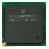
MPC8248VRPIEA Freescale Semiconductor, MPC8248VRPIEA Datasheet - Page 59

MPC8248VRPIEA
Manufacturer Part Number
MPC8248VRPIEA
Description
IC MPU POWERQUICC II 516-PBGA
Manufacturer
Freescale Semiconductor
Series
PowerQUICC IIr
Datasheet
1.MPC8248VRMIBA.pdf
(60 pages)
Specifications of MPC8248VRPIEA
Processor Type
MPC82xx PowerQUICC II 32-bit
Speed
300MHz
Voltage
1.5V
Mounting Type
Surface Mount
Package / Case
516-PBGA
Processor Series
MPC8xxx
Core
603e
Data Bus Width
32 bit
Maximum Clock Frequency
300 MHz
Operating Supply Voltage
1.4 V to 1.6 V
Maximum Operating Temperature
+ 105 C
Mounting Style
SMD/SMT
Data Ram Size
4 KB
Minimum Operating Temperature
0 C
Number Of Programmable I/os
14
Program Memory Size
16 KB
Program Memory Type
EEPROM
Core Size
32 Bit
Cpu Speed
300MHz
Embedded Interface Type
I2C, JTAG, SPI, UART
Digital Ic Case Style
BGA
No. Of Pins
516
Rohs Compliant
Yes
For Use With
CWH-PPC-8248N-VE - KIT EVAL SYSTEM QUICCSTART 8248
Lead Free Status / RoHS Status
Lead free / RoHS Compliant
Features
-
Lead Free Status / Rohs Status
Lead free / RoHS Compliant
Available stocks
Company
Part Number
Manufacturer
Quantity
Price
Company:
Part Number:
MPC8248VRPIEA
Manufacturer:
Freescale Semiconductor
Quantity:
135
Company:
Part Number:
MPC8248VRPIEA
Manufacturer:
Freescale Semiconductor
Quantity:
10 000
Freescale Semiconductor
Revision
0.2
0.1
0
12/2003
9/2003
5/2003
Date
•
•
•
•
•
•
•
•
• Sections 4.1–4.5 and 4.7 on thermal characteristics: New
•
• Addition of “Note: Temperature Reflow for the VR Package" on page 55
•
•
•
•
• Addition of the MPC8271 and the MPC8247 (these devices do not have a security engine)
•
•
• Modification of note 1 for
•
•
• Addition of ZQ package code to
NDA release
MPC8272 PowerQUICC II™ Family Hardware Specifications, Rev. 2
Table
Table
Table
Table
Table 5
CPCI_HS_ES to PCI_REQ1 (AF14)
CPCI_HS_LED to PCI_GNT1 (AE13)
CPCI_HS_ENUM to PCI_GNT2 (AF21)
Table 5
on other PowerQUICC II devices:
PCI_CFG0 (PCI_HOST_EN) (AC21)
PCI_CFG1 (PCI_ARB_EN) (AE22)
PCI_CFG2 (DLL_ENABLE) (AE23)
PCI_PAR (AF12)
PCI_FRAME (AD15)
PCI_TRDY(AF16)
PCI_IRDY (AF15)
PCI_STOP (AE15)
DEVSEL (AE14)
PCI_IDSEL (AC17)
PCI_PERR (AD14)
PCI_SERR (AD13)
PCI_REQ0–2 (AAE20, AF14, AB14)
PCI_GNT0–2 (AD20, AE13, AF21)
PCI_RST (AF22)
PCI_INTA (AE21)
PCI_C0-3 (AE12, AF13, AC15, AE18)
PCI_AD0-31
Table 5
PCI_ARB_EN (AE22)
Table
Section 7, “Clock Configuration
PCI_MODCK is a bit in the Hard Reset Configuration Word. It is not an input signal as it is in
the MPC8280 Family and MPC8260 Family.
Table
Table
Note 4 unchanged.
Table
Table
of note 1.
Table
Table
Table
to both CS5 and GND. AD8 is only assigned to CS5.
Table
Table 22. Document Revision History (continued)
1: New
2: New
4: Modification of VDD and VCCSYN to 1.45–1.60 V
5: Addition of note 2 regarding TRST and PORESET (see V
6: Addition of R
20: Addition of note 2 to TRST (E21) and PORESET (C24)
20: Removal of Thermal0 (D19) and Thermal1(J3). These pins are now “No connects.”
20: Removal of Spare0 (AD24). This pin is now a “No connect.” Note 5 unchanged.
20: Addition of PCI_MODE (AD22). This pin was previously listed as “Ground.” Addition
5: Addition of note 2 to V
5: Changed I
20: Addition of ball AD9 to GND. In rev 0 of this document, AD8 was listed as assigned
20: Addition of note 4 to Thermal0 (D19) and Thermal1(J3)
and
and
and
Table
Table
Table
20: Modification of PCI signal names for consistency with PCI signal names
20: Addition of muxed signals
20: Corrected assertion level (added “ “) PCI_HOST_EN (AC21) and
OL
θJT
for 60x signals to 6.0 mA
and note 4
Table
IH
16,
Modes”: Modification to first paragraph. Note that
Figure 15
Substantive Changes
Table
17,
Table
18, and
Table 19
IH
row of
Document Revision History
Table
5)
59


