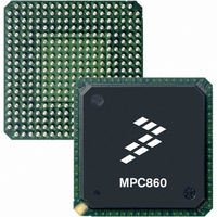
MPC866PZP133A Freescale Semiconductor, MPC866PZP133A Datasheet - Page 48

MPC866PZP133A
Manufacturer Part Number
MPC866PZP133A
Description
IC MPU POWERQUICC 133MHZ 357PBGA
Manufacturer
Freescale Semiconductor
Series
PowerQUICCr
Datasheet
1.MPC859DSLCVR50A.pdf
(96 pages)
Specifications of MPC866PZP133A
Processor Type
MPC8xx PowerQUICC 32-Bit
Speed
133MHz
Voltage
1.8V
Mounting Type
Surface Mount
Package / Case
357-PBGA
Processor Series
MPC8xx
Core
MPC8xx
Data Bus Width
32 bit
Maximum Clock Frequency
133 MHz
Maximum Operating Temperature
+ 95 C
Mounting Style
SMD/SMT
Minimum Operating Temperature
0 C
Family Name
MPC8xx
Device Core
PowerQUICC
Device Core Size
32b
Frequency (max)
133MHz
Instruction Set Architecture
RISC
Supply Voltage 1 (typ)
1.8V
Operating Supply Voltage (max)
1.9V
Operating Supply Voltage (min)
1.7V
Operating Temp Range
0C to 95C
Operating Temperature Classification
Commercial
Mounting
Surface Mount
Pin Count
357
Package Type
BGA
Core Size
32 Bit
Program Memory Size
24KB
Cpu Speed
133MHz
Digital Ic Case Style
BGA
No. Of Pins
357
Supply Voltage Range
1.7V To 1.9V
Rohs Compliant
No
Lead Free Status / RoHS Status
Contains lead / RoHS non-compliant
Features
-
Lead Free Status / Rohs Status
Lead free / RoHS Compliant
Available stocks
Company
Part Number
Manufacturer
Quantity
Price
Company:
Part Number:
MPC866PZP133A
Manufacturer:
FREESCAL
Quantity:
174
Company:
Part Number:
MPC866PZP133A
Manufacturer:
Freescale Semiconductor
Quantity:
10 000
CPM Electrical Characteristics
12 CPM Electrical Characteristics
This section provides the AC and DC electrical specifications for the communications processor module (CPM) of
the MPC866/859.
12.1 PIP/PIO AC Electrical Specifications
Table 16
48
1
Num
21
22
23
24
25
26
27
28
29
30
31
t3 = Specification 23
shows the PIP/PIO AC timings as shown in
Data-in setup time to STBI low
Data-In hold time to STBI high
STBI pulse width
STBO pulse width
Data-out setup time to STBO low
Data-out hold time from STBO high
STBI low to STBO low (Rx interlock)
STBI low to STBO high (Tx interlock)
Data-in setup time to clock high
Data-in hold time from clock high
Clock low to data-out valid (CPU writes data, control, or direction)
Signals
Signals
Signals
Output
Output
Output
TCK
Figure 40. Boundary Scan (JTAG) Timing Diagram
MPC866/MPC859 Hardware Specifications, Rev. 2
Characteristic
Table 16. PIP/PIO Timing
J92
J93
Figure 41
through
J95
Figure
J94
1 clk – 5ns
2.5 – t3
Min
1.5
7.5
All Frequencies
15
—
—
0
2
5
2
45.
1
J96
Max
25
—
—
—
—
—
—
—
—
—
2
Freescale Semiconductor
Unit
clk
clk
clk
clk
clk
clk
ns
ns
ns
ns
ns


