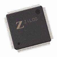
EZ80190AZ050SG Zilog, EZ80190AZ050SG Datasheet - Page 79

EZ80190AZ050SG
Manufacturer Part Number
EZ80190AZ050SG
Description
IC WEBSERVER 8 BIT 50MHZ 100LQFP
Manufacturer
Zilog
Datasheet
1.EZ80190AZ050SG.pdf
(221 pages)
Specifications of EZ80190AZ050SG
Processor Type
eZ80
Features
High Speed, Single-Cycle Instruction-Fetch
Speed
50MHz
Voltage
3.3V
Mounting Type
Surface Mount
Package / Case
100-LQFP
Processor Series
EZ80190x
Core
eZ80
Data Bus Width
8 bit
Program Memory Type
ROMLess
Data Ram Size
8 KB
Interface Type
I2C, IrDA, SPI, UART
Maximum Clock Frequency
50 MHz
Number Of Programmable I/os
32
Number Of Timers
6
Operating Supply Voltage
3 V to 3.6 V
Maximum Operating Temperature
+ 105 C
Mounting Style
SMD/SMT
Minimum Operating Temperature
- 40 C
Lead Free Status / RoHS Status
Lead free / RoHS Compliant
Other names
269-3866
EZ80190AZ050SG
EZ80190AZ050SG
Available stocks
Company
Part Number
Manufacturer
Quantity
Price
Company:
Part Number:
EZ80190AZ050SG
Manufacturer:
ZiLOG
Quantity:
135
- Current page: 79 of 221
- Download datasheet (4Mb)
PS006614-1208
UART Receiver
UART Modem Control
ister) is set to 1 and an interrupt is sent to the processor (if interrupts are enabled). The pro-
cessor can reset this interrupt by loading data into the UARTx_THR register, which clears
the transmitter interrupt.
The transmit shift register places the byte to be transmitted on the TXD signal serially. The
lsb of the byte to be transmitted is shifted out first and the msb is shifted out last. The con-
trol logic within the block adds the asynchronous communications protocol bits to the data
byte being transmitted. The transmitter block obtains the parameters for the protocol from
the bits programmed through the UARTx_LCTL register. The TXD output is set to 1 if the
transmitter is idle (it does not contain any data to be transmitted).
The transmitter operates with the Baud Rate Generator (BRG) clock. The data bits are
placed on the TXD output one time every 16 BRG clock cycles. The transmitter block also
implements a parity generator and attaches the parity bit with the byte if programmed to
do so.
The receiver block controls data reception from the RXD signal. The receiver block
implements a receiver shift register, receiver line error condition monitoring logic and
receiver data ready logic. It also implements a parity checker.
The processor reads received data from UARTx_RBR, which is a Read Only register. The
condition of the UARTx_RBR register is monitored by the DR bit (bit 0 of the
UARTx_LSR register). The DR bit is set to 1 when a data byte is received and transferred
to the UARTx_RBR register from the receiver shift register. The DR bit is reset only when
the processor reads all received data bytes. If the number of bits received is less than eight,
the unused msbs of the data byte read are reset to 0.
The receiver uses the clock from the BRG input of the UZI for receiving data. This clock
must be 16 times the required baud rate. The receiver synchronizes the shift clock on the
falling edge of the RXD input start bit. It then receives a complete byte according to the
set parameters. The receiver also implements logic to detect framing errors, parity errors,
overrun errors, and break signals.
The modem control logic provides two outputs and four inputs for handshaking with the
modem. Any change in the modem status inputs, except RI, is detected. An interrupt can
then be generated. For RI, an interrupt is generated only when the trailing edge of the RI is
detected. The module also provides a loop mode for self-diagnostic purposes.
Universal Asynchronous Receiver/Transmitter
Product Specification
eZ80190
69
Related parts for EZ80190AZ050SG
Image
Part Number
Description
Manufacturer
Datasheet
Request
R

Part Number:
Description:
Communication Controllers, ZILOG INTELLIGENT PERIPHERAL CONTROLLER (ZIP)
Manufacturer:
Zilog, Inc.
Datasheet:

Part Number:
Description:
KIT DEV FOR Z8 ENCORE 16K TO 64K
Manufacturer:
Zilog
Datasheet:

Part Number:
Description:
KIT DEV Z8 ENCORE XP 28-PIN
Manufacturer:
Zilog
Datasheet:

Part Number:
Description:
DEV KIT FOR Z8 ENCORE 8K/4K
Manufacturer:
Zilog
Datasheet:

Part Number:
Description:
KIT DEV Z8 ENCORE XP 28-PIN
Manufacturer:
Zilog
Datasheet:

Part Number:
Description:
DEV KIT FOR Z8 ENCORE 4K TO 8K
Manufacturer:
Zilog
Datasheet:

Part Number:
Description:
CMOS Z8 microcontroller. ROM 16 Kbytes, RAM 256 bytes, speed 16 MHz, 32 lines I/O, 3.0V to 5.5V
Manufacturer:
Zilog, Inc.
Datasheet:

Part Number:
Description:
Low-cost microcontroller. 512 bytes ROM, 61 bytes RAM, 8 MHz
Manufacturer:
Zilog, Inc.
Datasheet:

Part Number:
Description:
Z8 4K OTP Microcontroller
Manufacturer:
Zilog, Inc.
Datasheet:

Part Number:
Description:
CMOS SUPER8 ROMLESS MCU
Manufacturer:
Zilog, Inc.
Datasheet:

Part Number:
Description:
SL1866 CMOSZ8 OTP Microcontroller
Manufacturer:
Zilog, Inc.
Datasheet:

Part Number:
Description:
SL1866 CMOSZ8 OTP Microcontroller
Manufacturer:
Zilog, Inc.
Datasheet:

Part Number:
Description:
OTP (KB) = 1, RAM = 125, Speed = 12, I/O = 14, 8-bit Timers = 2, Comm Interfaces Other Features = Por, LV Protect, Voltage = 4.5-5.5V
Manufacturer:
Zilog, Inc.
Datasheet:

Part Number:
Description:
Manufacturer:
Zilog, Inc.
Datasheet:


