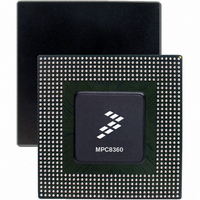
MPC8360VVAGDGA Freescale Semiconductor, MPC8360VVAGDGA Datasheet - Page 22

MPC8360VVAGDGA
Manufacturer Part Number
MPC8360VVAGDGA
Description
IC MPU POWERQUICC II PRO 740TBGA
Manufacturer
Freescale Semiconductor
Datasheet
1.MPC8360CZUAJDG.pdf
(108 pages)
Specifications of MPC8360VVAGDGA
Processor Type
MPC83xx PowerQUICC II Pro 32-Bit
Speed
400MHz
Voltage
1.2V
Mounting Type
Surface Mount
Package / Case
740-TBGA
Processor Series
MPC8xxx
Core
e300
Data Bus Width
32 bit
Development Tools By Supplier
MPC8360E-RDK
Maximum Clock Frequency
400 MHz
Maximum Operating Temperature
+ 105 C
Mounting Style
SMD/SMT
I/o Voltage
1.8 V, 2.5 V, 3.3 V
Minimum Operating Temperature
0 C
For Use With
MPC8360EA-MDS-PB - KIT APPLICATION DEV 8360 SYSTEMMPC8360E-RDK - BOARD REFERENCE DESIGN FOR MPC
Lead Free Status / RoHS Status
Lead free / RoHS Compliant
Features
-
Lead Free Status / Rohs Status
Lead free / RoHS Compliant
Available stocks
Company
Part Number
Manufacturer
Quantity
Price
Company:
Part Number:
MPC8360VVAGDGA
Manufacturer:
AVX
Quantity:
3 000
Company:
Part Number:
MPC8360VVAGDGA
Manufacturer:
Freescale Semiconductor
Quantity:
135
Company:
Part Number:
MPC8360VVAGDGA
Manufacturer:
Freescale Semiconductor
Quantity:
10 000
DDR and DDR2 SDRAM
Table 17
6.2
This section provides the AC electrical characteristics for the DDR and DDR2 SDRAM interface.
6.2.1
Table 18
GV
Table 19
GV
22
At recommended operating conditions with GV
At recommended operating conditions with GV
Input/output capacitance: DQ, DQS
Delta input/output capacitance: DQ, DQS
Note:
1. This parameter is sampled. GV
AC input low voltage
AC input high voltage
Note:
1. Maximum possible skew between a data strobe (MDQS[n]) and any corresponding bit of data (MDQ[8n + {0...7}] if 0 ≤ n ≤ 7)
AC input low voltage
AC input high voltage
or ECC (MECC[{0...7}] if n = 8).
MPC8360E/MPC8358E PowerQUICC II Pro Processor Revision 2.x TBGA Silicon Hardware Specifications, Rev. 4
DD
DD
(typ) = 1.8 V.
(typ) = 2.5 V.
provides the DDR capacitance when GV
provides the input AC timing specifications for the DDR2 SDRAM interface when
provides the input AC timing specifications for the DDR SDRAM interface when
DDR and DDR2 SDRAM AC Electrical Characteristics
DDR and DDR2 SDRAM Input AC Timing Specifications
Table 18. DDR2 SDRAM Input AC Timing Specifications for GV
Parameter
Parameter
Parameter/Condition
Table 17. DDR SDRAM Capacitance for GV
Table 19. DDR SDRAM Input AC Timing Specifications
DD
= 2.5 V ± 0.125 V, f = 1 MHz, T
DD
DD
of 1.8 V ± 5%.
of 2.5 V ± 5%.
Symbol
Symbol
V
V
V
V
IH
IL
IH
IL
DD
(typ) = 2.5 V.
Symbol
MV
MV
C
C
DIO
A
IO
REF
REF
= 25°C, V
Min
Min
—
—
+ 0.25
+ 0.31
OUT
DD
Min
—
6
(typ) = 2.5 V
= GV
MV
MV
DD
REF
REF
Max
DD
Max
/2, V
—
—
– 0.25
(typ) = 1.8 V
– 0.31
Max
0.5
OUT
8
(peak-to-peak) = 0.2 V.
Freescale Semiconductor
Unit
Unit
Unit
pF
pF
V
V
V
V
Notes
Notes
Notes
—
—
—
—
1
1


