MPC8347CVRAGDB Freescale Semiconductor, MPC8347CVRAGDB Datasheet - Page 74
MPC8347CVRAGDB
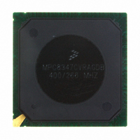
Manufacturer Part Number
MPC8347CVRAGDB
Description
IC MPU POWERQUICC II 620-PBGA
Manufacturer
Freescale Semiconductor
Series
PowerQUICC II PROr
Specifications of MPC8347CVRAGDB
Processor Type
MPC83xx PowerQUICC II Pro 32-Bit
Speed
400MHz
Voltage
1.2V
Mounting Type
Surface Mount
Package / Case
620-PBGA
Core Size
32 Bit
Program Memory Size
64KB
Cpu Speed
400MHz
Embedded Interface Type
I2C, SPI, USB, UART
Digital Ic Case Style
BGA
No. Of Pins
672
Rohs Compliant
Yes
Lead Free Status / RoHS Status
Lead free / RoHS Compliant
Features
-
Available stocks
Company
Part Number
Manufacturer
Quantity
Price
Company:

Part Number:
MPC8347CVRAGDB
Manufacturer:
FREESCA
Quantity:
13
Company:
Part Number:
MPC8347CVRAGDB
Manufacturer:
Freescale Semiconductor
Quantity:
10 000


Package and Pin Listings
74
LV
LV
V
OV
MVREF1
MVREF2
NC
Notes:
1. This pin is an open-drain signal. A weak pull-up resistor (1 kΩ) should be placed on this pin to OV
2. This pin is an open-drain signal. A weak pull-up resistor (2–10 kΩ) should be placed on this pin to OV
3. During reset, this output is actively driven rather than three-stated.
4. These JTAG pins have weak internal pull-up P-FETs that are always enabled.
5. This pin should have a weak pull-up if the chip is in PCI host mode. Follow the PCI specifications.
6. This pin must always be tied to GND.
7. This pin must always be left not connected.
8. Thermal sensitive resistor.
9. It is recommended that MDIC0 be tied to GRD using an 18 Ω resistor and MDIC1 be tied to DDR power using an 18 Ω resistor.
10.TSEC1_TXD[3] is required an external pull-up resistor. For proper functionality of the device, this pin must be pulled up or
11. A weak pull-up resistor (2–10 kΩ) should be placed on this pin to LV
12. For systems that boot from local bus (GPCM)-controlled NOR flash, a pullup on LGPL4 is required.
DD
DD
DD
actively driven high during a hard reset. No external pull-down resistors are allowed to be attached to this net.
DD
1
2
MPC8347EA PowerQUICC II Pro Integrated Host Processor Hardware Specifications, Rev. 11
Signal
Table 56. MPC8347EA (PBGA) Pinout Listing (continued)
B27, D3, D11, D19, E15, E23, F5, F8,
L25, M6, M9, M20, P5, P20, P23, R6,
L11, L18, L19, M10, M19, N10, N19,
T19, U10, U19, V10, V11, V18, V19,
F11, F14, F17, F20, G24, H23, H24,
K14, K15, K16, K17, K18, K19, L10,
J6, J14, J17, J18, K4, L9, L20, L23,
J11, J12, J15, K10, K11, K12, K13,
P9, P10, P19, R10, R19, R20, T10,
W11, W12, W13, W14, W15, W16,
No Connection
Package Pin Number
R9, R24, U23, V4, V6
V1, V2, V5
W17, W18
U20, W25
V20, Y23
AF19
AE10
DD1
.
Power for core
other standard
Ethernet, and
management
(2.5 V, 3.3 V)
interface I/O
three-speed
three-speed
PCI, 10/100
Ethernet #1
Ethernet #2
I/O (2.5 V,
Pin Type
Power for
Power for
Ethernet
and for
(1.2 V)
(3.3 V)
3.3 V)
—
I
I
DD
Freescale Semiconductor
.
DD
reference
reference
Supply
voltage
voltage
Power
LV
LV
OV
.
DDR
DDR
V
—
DD
DD
DD
DD
1
2
Notes
—
—
—
—
—
—
—
Related parts for MPC8347CVRAGDB
Image
Part Number
Description
Manufacturer
Datasheet
Request
R

Part Number:
Description:
Manufacturer:
Freescale Semiconductor, Inc
Datasheet:
Part Number:
Description:
Manufacturer:
Freescale Semiconductor, Inc
Datasheet:
Part Number:
Description:
Manufacturer:
Freescale Semiconductor, Inc
Datasheet:
Part Number:
Description:
Manufacturer:
Freescale Semiconductor, Inc
Datasheet:
Part Number:
Description:
Manufacturer:
Freescale Semiconductor, Inc
Datasheet:
Part Number:
Description:
Manufacturer:
Freescale Semiconductor, Inc
Datasheet:
Part Number:
Description:
Manufacturer:
Freescale Semiconductor, Inc
Datasheet:
Part Number:
Description:
Manufacturer:
Freescale Semiconductor, Inc
Datasheet:
Part Number:
Description:
Manufacturer:
Freescale Semiconductor, Inc
Datasheet:
Part Number:
Description:
Manufacturer:
Freescale Semiconductor, Inc
Datasheet:
Part Number:
Description:
Manufacturer:
Freescale Semiconductor, Inc
Datasheet:
Part Number:
Description:
Manufacturer:
Freescale Semiconductor, Inc
Datasheet:
Part Number:
Description:
Manufacturer:
Freescale Semiconductor, Inc
Datasheet:
Part Number:
Description:
Manufacturer:
Freescale Semiconductor, Inc
Datasheet:
Part Number:
Description:
Manufacturer:
Freescale Semiconductor, Inc
Datasheet: