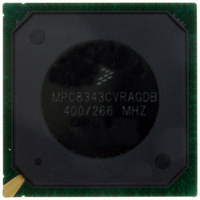
MPC8343CVRAGDB Freescale Semiconductor, MPC8343CVRAGDB Datasheet - Page 14

MPC8343CVRAGDB
Manufacturer Part Number
MPC8343CVRAGDB
Description
IC MPU PWRQUICC II 620-PBGA
Manufacturer
Freescale Semiconductor
Datasheet
1.MPC8343VRAGDB.pdf
(79 pages)
Specifications of MPC8343CVRAGDB
Processor Type
MPC83xx PowerQUICC II Pro 32-Bit
Speed
400MHz
Voltage
1.2V
Mounting Type
Surface Mount
Package / Case
620-PBGA
For Use With
CWH-PPC-8343N-VX - KIT EVAL SYSTEM QUICCSTART 8248CWH-PPC-8343N-VE - EVALUATION SYSTEM QUICC MPC8343E
Lead Free Status / RoHS Status
Lead free / RoHS Compliant
Features
-
Available stocks
Company
Part Number
Manufacturer
Quantity
Price
Company:
Part Number:
MPC8343CVRAGDB
Manufacturer:
Freescale Semiconductor
Quantity:
10 000
DDR and DDR2 SDRAM
Table 11
6
This section describes the DC and AC electrical specifications for the DDR SDRAM interface of the
MPC8343EA. Note that DDR SDRAM is GV
The AC electrical specifications are the same for DDR and DRR2 SDRAM.
6.1
Table 12
MPC8343EA when GV
14
Time for the MPC8343EA to turn on POR configuration signals with respect to the
negation of HRESET
Notes:
1. t
2. t
3. POR configuration signals consist of CFG_RESET_SOURCE[0:2] and CFG_CLKIN_DIV.
PLL lock times
DLL lock times
Notes:
1. DLL lock times are a function of the ratio between the output clock and the coherency system bus clock (csb_clk). A 2:1 ratio
2. The csb_clk is determined by the CLKIN and system PLL ratio. See
I/O supply voltage
to the CLKIN input, and PCI_SYNC_IN period depends on the value of CFG_CLKIN_DIV. See the MPC8349EA
PowerQUICC II Pro Integrated Host Processor Family Reference Manual.
PowerQUICC II Pro Integrated Host Processor Family Reference Manual.
results in the minimum and an 8:1 ratio results in the maximum.
PCI_SYNC_IN
CLKIN
DDR and DDR2 SDRAM
is the clock period of the input clock applied to CLKIN. It is valid only in PCI host mode. See the MPC8349EA
lists the PLL and DLL lock times.
provides the recommended operating conditions for the DDR2 SDRAM component(s) of the
DDR and DDR2 SDRAM DC Electrical Characteristics
Parameter/Condition
MPC8343EA PowerQUICC II Pro Integrated Host Processor Hardware Specifications, Rev. 10
is the clock period of the input clock applied to PCI_SYNC_IN. In PCI host mode, the primary clock is applied
The information in this document is accurate for revision 3.0 silicon and
later. For information on revision 1.1 silicon and earlier versions see the
MPC8343E PowerQUICC II Pro Integrated Host Processor Hardware
Specifications. See
Document,” for silicon revision level determination.
Table 12. DDR2 SDRAM DC Electrical Characteristics for GV
Parameter/Condition
Table 10. RESET Initialization Timing Specifications (continued)
DD
(typ) = 1.8 V
Parameter
Section 22.1, “Part Numbers Fully Addressed by This
Table 11. PLL and DLL Lock Times
.
Symbol
GV
DD
DD
(typ) = 2.5 V and DDR2 SDRAM is GV
NOTE
1.71
Min
7680
Section 19, “Clocking.”
Min
—
122,880
Max
Min
100
1
Max
1.89
DD
(typ) = 1.8 V
Max
—
csb_clk cycles
Freescale Semiconductor
Unit
μs
t
PCI_SYNC_IN
DD
Unit
V
Unit
(typ) = 1.8 V.
Notes
Notes
1, 2
Notes
—
1
1, 3


