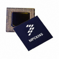
MPC8245LVV266D Freescale Semiconductor, MPC8245LVV266D Datasheet - Page 59

MPC8245LVV266D
Manufacturer Part Number
MPC8245LVV266D
Description
IC MPU 32BIT 266MHZ PPC 352-TBGA
Manufacturer
Freescale Semiconductor
Series
PowerQUICC IIr
Datasheet
1.MPC8245LZU266D.pdf
(68 pages)
Specifications of MPC8245LVV266D
Processor Type
MPC82xx PowerQUICC II 32-bit
Speed
266MHz
Voltage
1.8V
Mounting Type
Surface Mount
Package / Case
352-TBGA
Core Size
32 Bit
Program Memory Size
32KB
Cpu Speed
266MHz
Embedded Interface Type
I2C, UART
Digital Ic Case Style
TBGA
No. Of Pins
352
Supply Voltage Range
1.7V To 2.1V
Rohs Compliant
Yes
Lead Free Status / RoHS Status
Lead free / RoHS Compliant
Features
-
Available stocks
Company
Part Number
Manufacturer
Quantity
Price
Company:
Part Number:
MPC8245LVV266D
Manufacturer:
Freescal
Quantity:
672
Company:
Part Number:
MPC8245LVV266D
Manufacturer:
Freescale Semiconductor
Quantity:
10 000
Part Number:
MPC8245LVV266D
Manufacturer:
FREESCALE
Quantity:
20 000
Freescale Semiconductor
Revision
0.4
0.3
Date
—
—
Section 1.2—Changed Features list (format) to match with the features list of the MPC8245 Integrated
Processor Reference Manual.
Section 1.4.1.2—Updated Table 2 to include 1.8 ± 100mV numbers.
Section 1.4.3—Changed Table 7 to include new part offerings of 333 and 350 MHz. Added rows to
include VCO frequency ranges for all parts for both memory VCO and CPU VCO.
Section 1.4.1.5—Updated power consumption table to include 1.8 V (V
numbers.
Section 1.4.3—Updated Table 7 to include higher frequency offerings and CPU VCO frequency range.
Section 1.4.3.1—Changed lettering to caps for DLL_EXTEND and DLL_MAX_DELAY in graph
description section.
Section 1.4.3.2—Changed name of item 11 from T
T
Section 1.6—Updated notes in Table 17. Included minimum and maximum VCO numbers for memory
VCO. Changed Note 13 for location of PLL_CFG[0:4] to correct bits location. Bits 7–4 of register offset
<0xE2>. Added Table 18 to cover PLL configuration of higher frequency part offerings.
Section: 1.7—Changed frequency ranges for reference numbers 0, 9, 10, and 17, for the 300-MHz part
to include the higher memory bus frequencies when operating at lower CPU bus frequencies. Added
Table 18 to include PLL configurations for the 333 MHz and the 350 MHz CPU part offerings. Added
VCO multipliers in Tables 17 and 18.
Section 1.7.8—Changed T
SYNC_IN to sys_logic_clk Offset Time.”
Section 1.7.10—Added vendor (Cool Innovations, Inc.) to list of heat sink vendors.
Section 1.4.1.5—Changed Max-FP value for 33/133/266 of Table 5 from 2.3 to 2.1 watts to represent
characterization data. Changed Note 4 to say V
Changed numbers for maximum I/O power supplies for OV
data.
Section 1.4.3.1—Added four graphs (Figures 5–8) and description for DLL Locking Range vs.
Frequency of Operation to replace Figure 5 of Rev 0.2 document.
Section 1.4.3.2—Added row (item 11: T
include offset change requirement.
Section 1.5.3—Changed Note 4 of PLL_CFG pins in Table 16 to Note 20.
Section 1.7.2—Added diode (MUR420) to Figure 27, Voltage Sequencing Circuit, to compensate for
voltage extremes in design.
Section 1.7.5—Added sentence with regards to SDRAM_SYNC_IN to PCI_SYNC_IN timing
requirement (T
Section 1.7.8—Mention of T
and the MPC8245.
os
—SDRAM_SYNC_IN to sys_logic_clk Offset Time. Changed name to T
MPC8245 Integrated Processor Hardware Specifications, Rev. 10
Table 19. Revision History Table (continued)
su
) as a connection recommendation.
su
su
—SDRAM_SYNC_IN to PCI_SYNC_IN Time to T
offset timing and driver capability differences between the MPC8240
Substantive Change(s)
su
—SDRAM_SYNC_IN to PCI_SYNC_IN timing) to Table 9 to
DD
su
= 2.1 for power measurements (for 2-V part).
—SDRAM_SYNC_IN to PCI_SYNC_IN Time to
DD
and GV
DD
DD
to represent characterization
) and higher frequency
os
Document Revision History
in Note 7 as well.
os
—SDRAM_
59


