IS80C286-20 Intersil, IS80C286-20 Datasheet - Page 4
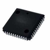
IS80C286-20
Manufacturer Part Number
IS80C286-20
Description
IC CPU 16BIT 5V 20MHZ 68-PLCC
Manufacturer
Intersil
Datasheet
1.CS80C286-12.pdf
(60 pages)
Specifications of IS80C286-20
Processor Type
80C286 16-Bit
Speed
20MHz
Voltage
5V
Mounting Type
Surface Mount
Package / Case
68-PLCC
Lead Free Status / RoHS Status
Contains lead / RoHS non-compliant
Features
-
Available stocks
Company
Part Number
Manufacturer
Quantity
Price


Pin Descriptions
SYMBOL
D
A
S1, S0
15
23
BHE
CLK
- D
- A
0
0
NUMBER
36 - 51
10 - 28
32 - 43
7 - 8
PIN
4, 5
31
1
The following pin function descriptions are for the 80C286 microprocessor.
TYPE
I/O
O
O
O
I
SYSTEM CLOCK: provides the fundamental timing for the 80C286 system. It is divided by two inside
the 80C286 to generate the processor clock. The internal divide-by-two circuitry can be synchro-
nized to an external clock generator by a LOW to HIGH transition on the RESET input.
DATA BUS: inputs data during memory, I/O, and interrupt acknowledge read cycles; outputs data
during memory and I/O write cycles. The data bus is active HIGH and is held at high impedance to
the last valid logic level during bus hold acknowledge.
ADDRESS BUS: outputs physical memory and I/O port addresses. A
transfers. A
bus is active High and floats to three-state off during bus hold acknowledge.
BUS HIGH ENABLE: indicates transfer of data on the upper byte of the data bus, D
oriented devices assigned to the upper byte of the data bus would normally use BHE to condition chip
select functions. BHE is active LOW and floats to three-state OFF during bus hold acknowledge.
BUS CYCLE STATUS: indicates initiation of a bus cycle and along with M/IO and COD/lNTA, de-
fines the type of bus cycle. The bus is in a T
active LOW and are held at a high impedance logic one during bus hold acknowledge.
COD/INTA
BHE VALUE
1(HIGH)
0(LOW)
0
0
0
0
0
0
0
1
1
1
1
1
1
1
0
0
0
1
1
is LOW when data is to be transferred on pins D
M/IO
0
0
0
0
1
1
1
1
0
0
0
1
1
1
1
0
80C286
A
80C286 BUS CYCLE STATUS DEFINITION
0
S1
0
0
1
1
0
0
1
1
0
0
1
1
0
0
1
1
4
VALUE
0
1
0
1
BHE AND A
S0
0
1
0
1
0
1
0
1
0
1
0
1
0
1
0
1
DESCRIPTION
Interrupt acknowledge
Reserved
Reserved
None; not a status cycle
If A
Memory data read
Memory data write
None; not a status cycle
Reserved
I/O read
I/O write
None; not a status cycle
Reserved
Memory instruction read
Reserved
None; not a status cycle
Word transfer
Byte transfer on upper half of data bus (D
Byte transfer on lower half of data bus (D
Reserved
S
1
state whenever one or both are LOW. S1 and S0 are
= 1 then halt; else shutdown
0
ENCODINGS
BUS CYCLE INITIATED
7
- D
FUNCTION
0
(see table below). The address
23
- A
16
are LOW during I/O
15
7
15
- D
- D
- D
8
. Eight-bit
0
)
8
)
Related parts for IS80C286-20
Image
Part Number
Description
Manufacturer
Datasheet
Request
R

Part Number:
Description:
Intersil Corporation [CMOS Serial Controller Interface]
Manufacturer:
Intersil Corporation
Datasheet:
Part Number:
Description:
Manufacturer:
Intersil Corporation
Datasheet:
Part Number:
Description:
357-036-542-201 CARDEDGE 36POS DL .156 BLK LOPRO
Manufacturer:
Intersil Corporation
Datasheet:
Part Number:
Description:
1024-Word x 4-Bit LSI Static RAM
Manufacturer:
Intersil Corporation
Datasheet:
Part Number:
Description:
General Purpose NPN Transistor Arrays FN341.4
Manufacturer:
Intersil Corporation
Datasheet:
Part Number:
Description:
CMOS 16-Bit Microprocessor
Manufacturer:
Intersil Corporation
Datasheet:
Part Number:
Description:
Manufacturer:
Intersil Corporation
Datasheet:
Part Number:
Description:
Manufacturer:
Intersil Corporation
Datasheet:
Part Number:
Description:
Manufacturer:
Intersil Corporation
Datasheet:
Part Number:
Description:
Manufacturer:
Intersil Corporation
Datasheet:
Part Number:
Description:
CMOS 6-Bit Latch and Decoder Memory Interfaces
Manufacturer:
Intersil Corporation
Datasheet:
Part Number:
Description:
CA3046General Purpose NPN Transistor Arrays
Manufacturer:
Intersil Corporation
Datasheet:
Part Number:
Description:
Manufacturer:
Intersil Corporation
Datasheet:
Part Number:
Description:
TR909 DLC/FLC SLIC with Low Power Standby
Manufacturer:
Intersil Corporation
Datasheet:
Part Number:
Description:
Manufacturer:
Intersil Corporation
Datasheet: