MPC8540PX667LC Freescale Semiconductor, MPC8540PX667LC Datasheet - Page 11
MPC8540PX667LC
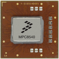
Manufacturer Part Number
MPC8540PX667LC
Description
IC MPU 32BIT 667MHZ 783-FCPBGA
Manufacturer
Freescale Semiconductor
Specifications of MPC8540PX667LC
Processor Type
MPC85xx PowerQUICC III 32-Bit
Speed
667MHz
Voltage
1.2V
Mounting Type
Surface Mount
Package / Case
783-FCPBGA
For Use With
MPC8548CDS - DEV TOOLS CDS FOR 8548MPC8540ADS-BGA - BOARD APPLICATION DEV 8540CWH-PPC-8540N-VE - KIT EVAL SYSTEM MPC8540
Lead Free Status / RoHS Status
Lead free / RoHS Compliant
Features
-
Available stocks
Company
Part Number
Manufacturer
Quantity
Price
Company:

Part Number:
MPC8540PX667LC
Manufacturer:
Freescale Semiconductor
Quantity:
10 000


3.2 On-Chip Memory Unit
The MPC8540 contains an internal 256-Kbyte memory array that can be configured as memory-mapped SRAM or
as a look-aside L2 cache. The array can also be divided into two 128-Kbyte arrays, one of which may be used as
cache and the other as SRAM.
The memory controller for this array connects to the core complex bus (CCB) and communicates through 128-bit
read and write buses to the e500 core and the MPC8540 system logic.
The on-chip memory unit contains:
3.2.1 On-Chip Memory as Memory-Mapped SRAM
When the on-chip memory is configured as an SRAM, the 256 Kbytes of memory can be configured to reside at any
aligned location in the memory map. It is byte-accessible and fully ECC-protected, using read-modify-write
transactions for sub-cacheline transactions. I/O devices can access the SRAM by marking transactions global so that
they are directed to the CCB.
3.2.2 On-Chip Memory as L2 Cache
The MPC8540 on-chip memory arrays include a 256-Kbyte data array, an address tag array, and a status array.
The data array is organized as 1024 sets of 8 cache lines. Each cache line size is 32 bytes. The replacement policy
in each eight-way set is governed by a pseudo-LRU algorithm. The data is protected with ECC, and the tag array is
protected by parity.
The L2 cache tags are non-blocking for efficient load/store and snooping operations. The L2 cache can be accessed
internally while a load miss is pending (allowing hits under misses). Subsequent to a load miss updating the memory,
loads or stores can occur to that line on the very next cycle.
Freescale Semiconductor
•
256 Kbytes of on-chip memory
— L2 cache partitioning is configurable
— SRAM operation is byte-accessible
— Data ECC on 64-bit boundaries (single-error correction, double-error detection)
— Tag parity (1 bit covering all tag bits)
— Cache mode supports instruction caching, data caching, or both
— External masters can force data to be allocated into the cache through programmed memory ranges or
— Separate locking for instructions and data so that locks can be set and cleared separately
— Supports locking the entire cache or selected lines
— Flash clearing done through writes to L2 configuration registers
— Locks for the entire cache may be set and cleared by accesses to memory-mapped control registers
– Can act as a 256-Kbyte L2 cache
– Array can be partitioned into 128-Kbyte L2 cache and 128-Kbyte memory mapped SRAM
– Can act as two 128-Kbyte memory-mapped SRAM arrays or a 256-Kbyte SRAM region
special transaction types
– Individual line locks are set and cleared through core-initiated instructions, by external reads or
writes, or by accesses to programmed memory ranges
–256-Kbyte array organized as 1024 eight-way sets of 32-byte cache lines
MPC8540 PowerQUICC III™ Integrated Host Processor Product Brief, Rev. 0.1
MPC8540 Architecture Overview
11
Related parts for MPC8540PX667LC
Image
Part Number
Description
Manufacturer
Datasheet
Request
R

Part Number:
Description:
Manufacturer:
Freescale Semiconductor, Inc
Datasheet:
Part Number:
Description:
Manufacturer:
Freescale Semiconductor, Inc
Datasheet:
Part Number:
Description:
Manufacturer:
Freescale Semiconductor, Inc
Datasheet:
Part Number:
Description:
Manufacturer:
Freescale Semiconductor, Inc
Datasheet:
Part Number:
Description:
Manufacturer:
Freescale Semiconductor, Inc
Datasheet:
Part Number:
Description:
Manufacturer:
Freescale Semiconductor, Inc
Datasheet:
Part Number:
Description:
Manufacturer:
Freescale Semiconductor, Inc
Datasheet:
Part Number:
Description:
Manufacturer:
Freescale Semiconductor, Inc
Datasheet:
Part Number:
Description:
Manufacturer:
Freescale Semiconductor, Inc
Datasheet:
Part Number:
Description:
Manufacturer:
Freescale Semiconductor, Inc
Datasheet:
Part Number:
Description:
Manufacturer:
Freescale Semiconductor, Inc
Datasheet:
Part Number:
Description:
Manufacturer:
Freescale Semiconductor, Inc
Datasheet:
Part Number:
Description:
Manufacturer:
Freescale Semiconductor, Inc
Datasheet:
Part Number:
Description:
Manufacturer:
Freescale Semiconductor, Inc
Datasheet:
Part Number:
Description:
Manufacturer:
Freescale Semiconductor, Inc
Datasheet: