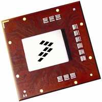
MPC8560VT667LC Freescale Semiconductor, MPC8560VT667LC Datasheet - Page 19

MPC8560VT667LC
Manufacturer Part Number
MPC8560VT667LC
Description
IC MPU POWERQUICC III 783-FCPBGA
Manufacturer
Freescale Semiconductor
Datasheet
1.MPC8560VT667LC.pdf
(36 pages)
Specifications of MPC8560VT667LC
Processor Type
MPC85xx PowerQUICC III 32-Bit
Speed
667MHz
Voltage
1.2V
Mounting Type
Surface Mount
Package / Case
783-FCPBGA
For Use With
MPC8560ADS-BGA - BOARD APPLICATION DEV 8560
Lead Free Status / RoHS Status
Lead free / RoHS Compliant
Features
-
Available stocks
Company
Part Number
Manufacturer
Quantity
Price
Company:
Part Number:
MPC8560VT667LC
Manufacturer:
Freescale Semiconductor
Quantity:
10 000
3.16 Address Map
The MPC8560 supports a flexible physical address map. Conceptually, the address map consists of local
space and external address space. The local address map is 4 Gbytes. The MPC8560 can be made part of a
larger system address space through the mapping of translation windows. This functionality is included in
the address translation and mapping units (ATMUs). Both inbound and outbound translation windows are
provided. The ATMUs allows the MPC8560 to be part of larger address maps such as the PCI 64-bit address
environment and the RapidIO environment.
3.17 OCeaN Switch Fabric
In order to reduce the strain on the core interconnects with the addition of new functional blocks in this
generation of the PowerQUICC family, an on-chip non-blocking crossbar switch fabric called OCeaN
(on-chip network) has been integrated to decrease contention, decrease latency, and increase bandwidth.
This revolutionary non-blocking crossbar fabric allows for full-duplex port connections at 128 Gbps
concurrent throughput and independent per-port transaction queuing and flow control.
Part IV Data Processing Overview
Protocol data units (PDUs) can navigate through the various MPC8560 I/O ports in three ways. With the
first method, data is processed by the MPC8560 CPM (as it is received and transmitted through the
UTOPIAs, MIIs, and TDMs associated with the CPM) and the local bus. In the second method, data is
received by any of the available I/O ports, sent through the on-chip switch fabric, and transmitted on the
target I/O port without the use of the ECM. The third method by which data can be routed from any I/O port
to any other I/O port is through the ECM.
4.1
In this case, the MPC8560 stores data in buffers that reside in SDRAM on the local bus. These buffers are
each referenced by a buffer descriptor (BD), which may reside in one of two tables—Rx-receive and
Tx-transmit—typically placed in DPRAM. The following is a general overview of how incoming data is
processed by the CPM (refer to Figure 3).
MOTOROLA
1. Rx data is decoded when it arrives on the I/O port; the PDU is delineated from the incoming data
2. Data is converted from its serial form into a parallel form and loaded into the Rx FIFO.
3. When the Rx FIFO is filled to a set threshold, the respective communication channel signals the
4. The CPM accesses the next available RxBD in the RxBD table (pointed to by a register in the
5. Data is finally moved from this temporary storage location to main memory through DMA
6. A CPU interrupt is instantiated to notify the core that a new packet has been received.
stream.
CPM for service.
channel’s parameter RAM table). The BD defines the main memory location where the data is to
be placed, as well as the length of this buffer. Data is then moved from the Rx FIFO to a temporary
storage location by the CPM.
transactions. The status and control bits of the BD are updated, and the BD is closed.
Processing Between the CPM and Local Bus
PRELIMINARY—SUBJECT TO CHANGE WITHOUT NOTICE
Integrated Communications Processor Product Brief
Freescale Semiconductor, Inc.
For More Information On This Product,
MPC8560 PowerQUICC III™
Go to: www.freescale.com
Address Map
19


