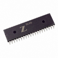
Z0840004PSC Zilog, Z0840004PSC Datasheet - Page 92

Z0840004PSC
Manufacturer Part Number
Z0840004PSC
Description
IC 4MHZ Z80 NMOS CPU 40-DIP
Manufacturer
Zilog
Datasheet
1.Z0840004PSC.pdf
(98 pages)
Specifications of Z0840004PSC
Processor Type
Z80
Features
NMOS
Speed
4MHz
Voltage
5V
Mounting Type
Through Hole
Package / Case
40-DIP (0.620", 15.75mm)
Lead Free Status / RoHS Status
Contains lead / RoHS non-compliant
Available stocks
Company
Part Number
Manufacturer
Quantity
Price
Company:
Part Number:
Z0840004PSC
Manufacturer:
ZILOG
Quantity:
2 000
Part Number:
Z0840004PSC
Manufacturer:
ZILOG
Quantity:
20 000
Part Number:
Z0840004PSC (Z80CPU)
Manufacturer:
ZILOG
Quantity:
20 000
Part Number:
Z0840004PSC(Z80CPU)
Manufacturer:
ZILOG
Quantity:
20 000
ZiLOG
ZAC03-0004
TERM
Develop:
Develop inspect:
Die:
Diffusion:
Dopant:
Dose:
Drain:
Dry Masking:
EDX:
EOS:
ESD:
Enhancement transistor:
Etch rate:
Evaporation:
Expose:
FAE:
Final Test:
DEFINITION
A chemical process that solidifies photoresist where it has been
exposed and removes it elsewhere (for negative resist) or vice versa
(for positive resist).
A visual check following dry masking to verify proper resist
patterning before etch, e.g., alignment and thickness are checked.
A single integrated circuit separated from the wafer on which it was
made; also called a chip.
The process of doping silicon by diffusing impurities from the
surface into the wafer at high temperature. Any region in the
silicon substrate doped by diffusion or by ion implant (e.g., source
and drain diffusions).
Any impurity intentionally introduced into silicon to control its
electronic behavior (e.g., Boron, Arsenic, and Phosphorus).
In ion implant, a measure of the amount of dopant implanted;
usually expressed in ions per square centimeter.
A highly doped region adjacent to a transistor currently carrying
channel. It carries electrons out of the transistor to the next circuit
element or conductor.
A process segment where a photoresist is spun onto the wafer, soft
baked, exposed, and developed to obtain a desired pattern ready for
etch or implant (see "wet masking”).
Energy Dispersive X-ray analysis. Normally uses electron beam
excitation in the scanning electron microscope.
Electrical overstress, common application failure mechanism.
Electrostatic discharge, common handling failure mechanism.
A MOSFET with a normally “off” channel; requires a positive
applied gate voltage to turn on (see “depletion transistor”).
The rate at which a given layer is etched off in a given standard
acid solution, expressed in Å/sec.
Deposition technique for Aluminum, Gold, and Chromium thin
films.
Expose a photoresist-coated wafer to light through a mask.
Field Application Engineer.
Measurement of assembled device performance. Products are
categorized by speed/power/performance criteria.
2002 Quality and Reliability Report
11- 3


