MC68EC020FG25 Freescale Semiconductor, MC68EC020FG25 Datasheet - Page 259
MC68EC020FG25
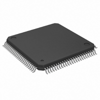
Manufacturer Part Number
MC68EC020FG25
Description
IC MPU 32 BIT 25MHZ 100-QFP
Manufacturer
Freescale Semiconductor
Datasheet
1.MC68EC020AA16.pdf
(306 pages)
Specifications of MC68EC020FG25
Processor Type
M680x0 32-Bit
Speed
25MHz
Voltage
5V
Mounting Type
Surface Mount
Package / Case
100-QFP
Lead Free Status / RoHS Status
Contains lead / RoHS non-compliant
Features
-
Available stocks
Company
Part Number
Manufacturer
Quantity
Price
Company:

Part Number:
MC68EC020FG25
Manufacturer:
FREESCALE
Quantity:
8 831
Company:
Part Number:
MC68EC020FG25
Manufacturer:
Freescale Semiconductor
Quantity:
10 000
Part Number:
MC68EC020FG25
Manufacturer:
MOTOROL
Quantity:
20 000


9.2 BYTE SELECT LOGIC FOR THE MC68020/EC020
The MC68020/EC020 architecture supports byte, word, and long-word operand transfers
to any 8-, 16-, or 32-bit data port, regardless of alignment. This feature allows the
programmer to write code that is not bus-width specific. When accessed, the peripheral or
memory subsystem reports its actual port size to the controller, and the MC68020/EC020
then dynamically sizes the data transfer accordingly, using multiple bus cycles when
necessary. The following paragraphs describe the generation of byte select control signals
that enable the dynamic bus sizing mechanism, the transfer of differently sized operands,
and the transfer of misaligned operands to operate correctly.
The following signals control the MC68020/EC020 operand transfer mechanism:
The need for byte select signals is best illustrated by an example. Consider a long-word
write cycle to an odd address in word-organized memory. The transfer requires three bus
cycles to complete. The first bus cycle transfers the most significant byte of the long word
on D23–D16. The second bus cycle transfers a word on D31–D16, and the last bus cycle
transfers the least significant byte of the original long word on D31–D24. To prevent
overwriting those bytes that are not used in these transfers, a unique byte data strobe
must be generated for each byte when using devices with 16- and 32-bit port widths.
For noncachable read cycles and all write cycles, the required active bytes of the data bus
for any given bus transfer are a function of the SIZ1, SIZ0 and A1, A0 outputs (see Table
9-1). Individual strobes or select signals can be generated by decoding these four signals
for every bus cycle. Devices residing on 8-bit ports can utilize DS or AS since there is only
one valid byte for any transfer.
MOTOROLA
The MC68020/EC020 assumes that 16-bit ports are situated on data lines D31–D16, and
that 8-bit ports are situated on data lines D31–D24. This ensures that the following logic
works correctly with the MC68020/EC020's on-chip internal-to-external data bus
multiplexer. Refer to Section 5 Bus Operation for more details on the dynamic bus sizing
mechanism.
DSACK1 , DSACK0 — Data transfer and size acknowledge signals. Driven by an
SIZ1, SIZ0
A1, A0
R/ W
— Address signals. The most significant byte of the operand to be
— Read/Write signal. Output of the MC68020/EC020. For byte
— Transfer size signals. Output of the MC68020/EC020. These
transferred is addressed directly.
indicate the number of bytes of an operand remaining to be
transferred during a given bus cycle.
select generation in MC68020/EC020 systems.
asynchronous port to indicate the actual bus width of
the port.
M68020 USER’S MANUAL
9- 5
Related parts for MC68EC020FG25
Image
Part Number
Description
Manufacturer
Datasheet
Request
R

Part Number:
Description:
Manufacturer:
Freescale Semiconductor, Inc
Datasheet:
Part Number:
Description:
Manufacturer:
Freescale Semiconductor, Inc
Datasheet:
Part Number:
Description:
Manufacturer:
Freescale Semiconductor, Inc
Datasheet:
Part Number:
Description:
Manufacturer:
Freescale Semiconductor, Inc
Datasheet:
Part Number:
Description:
Manufacturer:
Freescale Semiconductor, Inc
Datasheet:
Part Number:
Description:
Manufacturer:
Freescale Semiconductor, Inc
Datasheet:
Part Number:
Description:
Manufacturer:
Freescale Semiconductor, Inc
Datasheet:
Part Number:
Description:
Manufacturer:
Freescale Semiconductor, Inc
Datasheet:
Part Number:
Description:
Manufacturer:
Freescale Semiconductor, Inc
Datasheet:
Part Number:
Description:
Manufacturer:
Freescale Semiconductor, Inc
Datasheet:
Part Number:
Description:
Manufacturer:
Freescale Semiconductor, Inc
Datasheet:
Part Number:
Description:
Manufacturer:
Freescale Semiconductor, Inc
Datasheet:
Part Number:
Description:
Manufacturer:
Freescale Semiconductor, Inc
Datasheet:
Part Number:
Description:
Manufacturer:
Freescale Semiconductor, Inc
Datasheet:
Part Number:
Description:
Manufacturer:
Freescale Semiconductor, Inc
Datasheet: