MC68EC020FG25 Freescale Semiconductor, MC68EC020FG25 Datasheet - Page 80
MC68EC020FG25
Manufacturer Part Number
MC68EC020FG25
Description
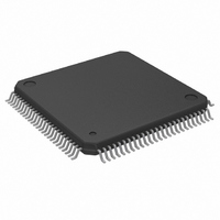
IC MPU 32 BIT 25MHZ 100-QFP
Manufacturer
Freescale Semiconductor
Datasheet
1.MC68EC020AA16.pdf
(306 pages)
Specifications of MC68EC020FG25
Processor Type
M680x0 32-Bit
Speed
25MHz
Voltage
5V
Mounting Type
Surface Mount
Package / Case
100-QFP
Lead Free Status / RoHS Status
Contains lead / RoHS non-compliant
Features
-
Available stocks
Company
Part Number
Manufacturer
Quantity
Price
Company:

Part Number:
MC68EC020FG25
Manufacturer:
FREESCALE
Quantity:
8 831
Company:
Part Number:
MC68EC020FG25
Manufacturer:
Freescale Semiconductor
Quantity:
10 000
Part Number:
MC68EC020FG25
Manufacturer:
MOTOROL
Quantity:
20 000


5.3.2 Write Cycle
During a write cycle, the processor transfers data to memory or a peripheral device.
Figure 5-24 is a flowchart of a write cycle operation for a long-word transfer. Figures 5-25–
5-28 are write cycle timing diagrams in terms of clock periods. Figure 5-25 shows two
write cycles (between two read cycles with no idle time in between) for a 32-bit port.
Figure 5-26 shows byte and word write cycles to a 32-bit port. Figure 5-27 shows a long-
word write cycle to an 8-bit port. Figure 5-28 shows a long-word write cycle to a 16-bit
port.
MOTOROLA
**
**
*
*
*
*
This step does not apply to the MC68EC020.
For the MC68EC020, A23–A0.
1) ASSERT ECS/OCS FOR ONE-HALF CLOCK
2) DRIVE ADDRESS ON A31–A0
3) DRIVE FUNCTION CODES ON FC2–FC0
4) DRIVE SIZ1, SIZ0 (FOUR BYTES)
5) SET R/W TO WRITE
6) ASSERT AS
7) ASSERT DBEN
8) DRIVE DATA LINES D31–D0
9) ASSERT DS
1) NEGATE AS AND DS
2) REMOVE DATA FROM D31–D0
3) NEGATE DBEN
TERMINATE OUTPUT TRANSFER
START NEXT CYCLE
ADDRESS DEVICE
PROCESSOR
Figure 5-24. Write Cycle Flowchart
M68020 USER’S MANUAL
1) DECODE ADDRESS
2) STORE DATA FROM D31–D0
3) ASSERT DSACK1/DSACK0
1) NEGATE DSACK1/DSACK0
EXTERNAL DEVICE
TERMINATE CYCLE
ACCEPT DATA
5- 33
Related parts for MC68EC020FG25
Image
Part Number
Description
Manufacturer
Datasheet
Request
R

Part Number:
Description:
Manufacturer:
Freescale Semiconductor, Inc
Datasheet:
Part Number:
Description:
Manufacturer:
Freescale Semiconductor, Inc
Datasheet:
Part Number:
Description:
Manufacturer:
Freescale Semiconductor, Inc
Datasheet:
Part Number:
Description:
Manufacturer:
Freescale Semiconductor, Inc
Datasheet:
Part Number:
Description:
Manufacturer:
Freescale Semiconductor, Inc
Datasheet:
Part Number:
Description:
Manufacturer:
Freescale Semiconductor, Inc
Datasheet:
Part Number:
Description:
Manufacturer:
Freescale Semiconductor, Inc
Datasheet:
Part Number:
Description:
Manufacturer:
Freescale Semiconductor, Inc
Datasheet:
Part Number:
Description:
Manufacturer:
Freescale Semiconductor, Inc
Datasheet:
Part Number:
Description:
Manufacturer:
Freescale Semiconductor, Inc
Datasheet:
Part Number:
Description:
Manufacturer:
Freescale Semiconductor, Inc
Datasheet:
Part Number:
Description:
Manufacturer:
Freescale Semiconductor, Inc
Datasheet:
Part Number:
Description:
Manufacturer:
Freescale Semiconductor, Inc
Datasheet:
Part Number:
Description:
Manufacturer:
Freescale Semiconductor, Inc
Datasheet:
Part Number:
Description:
Manufacturer:
Freescale Semiconductor, Inc
Datasheet: