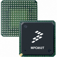
MPC852TVR50 Freescale Semiconductor, MPC852TVR50 Datasheet - Page 2

MPC852TVR50
Manufacturer Part Number
MPC852TVR50
Description
IC MPU POWERQUICC 50MHZ 256-PBGA
Manufacturer
Freescale Semiconductor
Datasheet
1.MPC852TVR100.pdf
(80 pages)
Specifications of MPC852TVR50
Processor Type
MPC8xx PowerQUICC 32-Bit
Speed
50MHz
Voltage
1.8V
Mounting Type
Surface Mount
Package / Case
256-PBGA
Lead Free Status / RoHS Status
Contains lead / RoHS non-compliant
Features
-
Available stocks
Company
Part Number
Manufacturer
Quantity
Price
Company:
Part Number:
MPC852TVR50
Manufacturer:
FREESCAL
Quantity:
465
Company:
Part Number:
MPC852TVR50A
Manufacturer:
FREESCALE
Quantity:
662
Company:
Part Number:
MPC852TVR50A
Manufacturer:
FREESCAL
Quantity:
319
Company:
Part Number:
MPC852TVR50A
Manufacturer:
Freescale Semiconductor
Quantity:
10 000
Part Number:
MPC852TVR50A
Manufacturer:
FREESCALE
Quantity:
20 000
Features
2 Features
The MPC852T is comprised of three modules that each use the 32-bit internal bus: the MPC8xx core, the system
integration unit (SIU), and the communication processor module (CPM).
diagram.
The following list summarizes the key MPC852T features:
2
•
•
•
•
•
•
•
•
Embedded MPC8xx core up to 100 MHz
Maximum frequency operation of the external bus is 66 MHz
— The 50 MHz / 66 MHz core frequencies support both 1:1 and 2:1 modes.
— The 80 MHz / 100 MHz core frequencies support 2:1 mode only.
Single-issue, 32-bit core (compatible with the PowerPC architecture definition) with 32 32-bit
general-purpose registers (GPRs)
— The core performs branch prediction with conditional prefetch, without conditional execution.
— 4-Kbyte data cache and 4-Kbyte instruction cache
— MMUs with 32-entry TLB, fully associative instruction, and data TLBs
— MMUs support multiple page sizes of 4, 16, and 512 Kbytes, and 8 Mbytes; 16 virtual address spaces,
Up to 32-bit data bus (dynamic bus sizing for 8, 16, and 32 bits)
32 address lines
Memory controller (eight banks)
— Contains complete dynamic RAM (DRAM) controller
— Each bank can be a chip select or RAS to support a DRAM bank
— Up to 30 wait states programmable per memory bank
— Glueless interface to DRAM, SIMMS, SRAM, EPROMs, Flash EPROMs, and other memory devices
— DRAM controller-programmable to support most size and speed memory interfaces
— Four CAS lines, four WE lines, and one OE line
— Boot chip-select available at reset (options for 8-, 16-, or 32-bit memory)
— Variable block sizes (32 Kbytes–256 Mbytes)
— Selectable write protection
— On-chip bus arbitration logic
Fast Ethernet Controller (FEC)
General-purpose timers
— Two 16-bit timers or one 32-bit timer
— Gate mode can enable or disable counting.
— Interrupt can be masked on reference match and event capture.
– 4-Kbyte instruction cache is two-way, set-associative with 128 sets.
– 4-Kbyte data cacheis two-way, set-associative with 128 sets.
– Cache coherency for both instruction and data caches is maintained on 128-bit (4-word) cache
– Caches are physically addressed, implement a least recently used (LRU) replacement algorithm, and
and 16 protection groups
blocks.
are lockable on a cache block basis.
MPC852T Hardware Specifications, Rev. 3.1
Figure 1
shows the MPC852T block
Freescale Semiconductor


