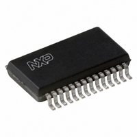
UDA1345TS/N2,112 NXP Semiconductors, UDA1345TS/N2,112 Datasheet - Page 8

UDA1345TS/N2,112
Manufacturer Part Number
UDA1345TS/N2,112
Description
IC AUDIO CODEC 28-SSOP
Manufacturer
NXP Semiconductors
Type
Stereo Audior
Datasheet
1.UDA1345TSN2118.pdf
(29 pages)
Specifications of UDA1345TS/N2,112
Package / Case
28-SSOP (0.200", 5.30mm Width)
Data Interface
Serial
Resolution (bits)
24 b
Number Of Adcs / Dacs
2 / 2
Sigma Delta
Yes
S/n Ratio, Adcs / Dacs (db) Typ
94 / 98
Voltage - Supply, Analog
2.4 V ~ 3.6 V
Voltage - Supply, Digital
2.4 V ~ 3.6 V
Operating Temperature
-40°C ~ 85°C
Mounting Type
Surface Mount
Number Of Adc Inputs
2
Number Of Dac Outputs
2
Conversion Rate
100 KSPS
Interface Type
Serial (I2S) or L3
Resolution
24 bit
Operating Supply Voltage
2.4 V to 3.6 V
Maximum Operating Temperature
+ 85 C
Mounting Style
SMD/SMT
Minimum Operating Temperature
- 40 C
Number Of Channels
2 ADC / 2 DAC
Supply Current
10 mA
Lead Free Status / RoHS Status
Lead free / RoHS Compliant
Lead Free Status / RoHS Status
Lead free / RoHS Compliant, Lead free / RoHS Compliant
Other names
568-1157-5
935266777112
UDA1345TSDB
935266777112
UDA1345TSDB
Available stocks
Company
Part Number
Manufacturer
Quantity
Price
Company:
Part Number:
UDA1345TS/N2,112
Manufacturer:
ON
Quantity:
12 000
NXP Semiconductors
7
The UDA1345TS accommodates slave mode only, this
means that in all applications the system devices must
provide the system clocks (being the system clock itself
and the digital audio interface signals).
The system clock must be locked in frequency to the audio
digital interface input signals.
The BCK clock can be up to 128f
BCK frequency is 128 times the Word Select (WS)
frequency or less: f
Important: the WS edge MUST fall on the negative edge
of the BCK at all times for proper operation of the digital I/O
data interface.
Note: the sampling frequency range is from 8 to 100 kHz,
however for the 512f
from 8 to 55 kHz.
2002 May 28
handbook, halfpage
Economy audio CODEC
FUNCTIONAL DESCRIPTION
V DDA(ADC)
V SSA(ADC)
SYSCLK
V ADCN
V ADCP
V ref(A)
V DDD
V SSD
VINR
VINL
MC1
MP1
MP2
MP3
Fig.2 Pin configuration.
BCK
10
11
12
13
14
1
2
3
4
5
6
7
8
9
s
clock mode the sampling range is
≤ 128 × f
UDA1345TS
MGS876
WS
s
, or in other words the
.
19
18
17
16
15
28
27
26
25
24
23
22
21
20
V ref(D)
V SSO
VOUTL
V DDO
VOUTR
V DDA(DAC)
V SSA(DAC)
MC2
MP5
DATAI
DATAO
WS
BCK
MP4
8
7.1
The stereo ADC of the UDA1345TS consists of two
5th-order Sigma-Delta modulators. They have a modified
Ritchie-coder architecture in a differential switched
capacitor implementation. The oversampling ratio is 64.
7.2
The analog front-end is equipped with a selectable 0 dB or
6 dB gain block (the pin to select this mode is given in
Section 7.10). This block can be used in applications in
which both 1 V (RMS) and 2 V (RMS) input signals can be
input to the UDA1345TS.
In applications in which a 2 V (RMS) input signal is used,
a 12 kΩ resistor must be used in series with the input of the
ADC. This forms a voltage divider together with the internal
ADC resistor and ensures that only 1 V (RMS) maximum
is input to the IC. Using this application for a 2 V (RMS)
input signal, the switch must be set to 0 dB. When a
1 V (RMS) input signal is input to the ADC in the same
application, the gain switch must be set to 6 dB.
An overview of the maximum input voltages allowed
against the presence of an external resistor and the setting
of the gain switch is given in Table 1; the power supply
voltage is assumed to be 3 V.
Table 1 Application modes using input gain stage
7.3
The decimation from 64f
The first stage realizes a 4th-order
This filter decreases the sample rate by 8. The second
stage consists of 2 half-band filters and a recursive filter,
each decimating by a factor of 2.
Present
Present
Absent
Absent
RESISTOR
(12 kΩ)
Decimation filter (ADC)
Analog-to-Digital Converter (ADC)
Analog front-end
INPUT GAIN
s
SWITCH
to 1fs is performed in two stages.
0 dB
6 dB
0 dB
6 dB
sin x
----------- -
UDA1345TS
Product specification
x
characteristic.
0.5 V (RMS)
MAXIMUM
VOLTAGE
2 V (RMS)
1 V (RMS)
1 V (RMS)
INPUT


