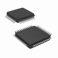
LM4549BVHX/NOPB National Semiconductor, LM4549BVHX/NOPB Datasheet - Page 18

LM4549BVHX/NOPB
Manufacturer Part Number
LM4549BVHX/NOPB
Description
IC AUDIO CODEC 2MULTICH 48-LQFP
Manufacturer
National Semiconductor
Type
Audio Codec '97r
Datasheet
1.LM4549BVHXNOPB.pdf
(28 pages)
Specifications of LM4549BVHX/NOPB
Data Interface
Serial
Resolution (bits)
18 b
Number Of Adcs / Dacs
2 / 2
Sigma Delta
Yes
Dynamic Range, Adcs / Dacs (db) Typ
90 / 89
Voltage - Supply, Analog
4.2 V ~ 5.5 V
Voltage - Supply, Digital
3.3 V ~ 5.5 V
Operating Temperature
-40°C ~ 85°C
Mounting Type
Surface Mount
Package / Case
48-LQFP
Lead Free Status / RoHS Status
Lead free / RoHS Compliant
Other names
LM4549BVHX
Available stocks
Company
Part Number
Manufacturer
Quantity
Price
Company:
Part Number:
LM4549BVHX/NOPB
Manufacturer:
TI/NS
Quantity:
25
Company:
Part Number:
LM4549BVHX/NOPB
Manufacturer:
Texas Instruments
Quantity:
10 000
Part Number:
LM4549BVHX/NOPB
Manufacturer:
TI/德州仪器
Quantity:
20 000
www.national.com
AC Link Serial Interface Protocol
SDATA_OUT: Slot 0 – Tag Phase
The first bit of Slot 0 is designated the "Valid Frame" bit. If
this bit is 1, it indicates that the current Output Frame con-
tains at least one slot of valid data and the LM4549B will
check further tag bits for valid data in the expected Data
Slots. With the codec in Primary mode, a controller will
indicate valid data in a slot by setting the associated tag bit
equal to 1. Since it is a two channel codec the LM4549B can
only receive data from four slots in a given frame and so only
checks the valid-data bits for 4 slots. In Primary mode these
tag bits are for: slot 1 (Command Address), slot 2 (Command
Data), slot 3 (PCM data for left DAC) and slot 4 (PCM data
for right DAC).
The last two bits in the Tag contain the Codec ID used to
select the target codec to receive the frame in multiple codec
systems. When the frame is being sent to a codec in one of
the Secondary modes the controller does not use bits 14 and
13 to indicate valid Command Address and Data in slots 1
and 2. Instead, this role is performed by the Codec ID bits –
operation of the Extended AC Link assumes that the control-
ler would not access a secondary codec unless it was pro-
viding valid Command Address and/or Data. When in one of
the secondary modes the LM4549B only checks the tag bits
for the Codec ID and for valid data in the two audio data slots
3 & 4.
When sending an Output Frame to a Secondary mode co-
dec, a controller should set tag bits 14 and 13 to zero.
(Continued)
Bit
15
14
13
12
FIGURE 5. Start of AC Link Output Frame
Control register
Control register
Left DAC data
Description
Valid Frame
in Slot 3
address
data
SLOT 0, OUTPUT FRAME
1 = Valid data in at least one
1 = Valid Control Address in
1 = Valid Control Data in Slot
1 = Valid PCM Data in Slot 3
slot.
Slot 1 (Primary codec
only)
2 (Primary codec only)
(Primary & all Secondary
modes)
Comment
20123505
18
SDATA_OUT: Slot 1 – Read/Write, Control Address
Slot 1 is used by a controller to indicate both the address of
a target register in the LM4549B and whether the access
operation is a register read or register write. The MSB of slot
1 (bit 19) is set to 1 to indicate that the current access
operation is ’read’. Bits 18 through 12 are used to specify the
7-bit register address of the read or write operation. The
least significant twelve bits are reserved and should be
stuffed with zeros by the AC ’97 controller.
SDATA_OUT: Slot 2 – Control Data
Slot 2 is used to transmit 16-bit control data to the LM4549B
when the access operation is ’write’. The least significant
four bits should be stuffed with zeros by the AC ’97 controller.
If the access operation is a register read, the entire slot, bits
19 through 0 should be stuffed with zeros.
SDATA_OUT: Slots 3 & 4 – PCM Playback Left/Right
Channels
Slots 3 and 4 are 20-bit fields used to transmit PCM data to
the left and right channels of the stereo DAC for all codec
Primary and Secondary modes. Any unused bits should be
stuffed with zeros. The LM4549B DACs have 18-bit resolu-
tion and will therefore use the 18 MSBs of the 20-bit PCM
data (MSB justified).
18:12
10:2
Bits
11:0
Bits
19:4
Bit
1,0
3:0
11
19
Right DAC data
Register Write
Description
Description
Description
Read/Write
(ID1, ID0)
Reserved
Reserved
Not Used
Codec ID
in Slot 4
Register
Address
Control
Data
SLOT 1, OUTPUT FRAME
SLOT 2, OUTPUT FRAME
Controller should stuff these
slots with “0”s
The codec ID is used in a
multi-codec system to identify
the target Secondary codec for
the Control Register address
and/or data sent in the Output
Frame
1 = Read
0 = Write
Identifies the Status/Command
register for read/write
Controller should set to "0"
Controller should stuff with
zeros if operation is “read”
Set to "0"
1 = Valid PCM Data in Slot 4
(Primary & all Secondary
modes)
Comment
Comment
Comment


