SC18IS601IBS,151 NXP Semiconductors, SC18IS601IBS,151 Datasheet - Page 5
SC18IS601IBS,151
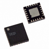
Manufacturer Part Number
SC18IS601IBS,151
Description
IC SPI TO I2C BUS 24-HVQFN
Manufacturer
NXP Semiconductors
Datasheet
1.SC18IS600IBS151.pdf
(30 pages)
Specifications of SC18IS601IBS,151
Package / Case
24-VQFN Exposed Pad, 24-HVQFN, 24-SQFN, 24-DHVQFN
Controller Type
I²C Bus Controller
Interface
SPI
Voltage - Supply
2.4 V ~ 3.6 V
Current - Supply
11mA
Operating Temperature
-40°C ~ 85°C
Mounting Type
Surface Mount
Maximum Operating Frequency
12 MHz
Maximum Operating Temperature
+ 85 C
Minimum Operating Temperature
- 40 C
Mounting Style
SMD/SMT
Supply Voltage (max)
3.6 V
Supply Voltage (min)
2.4 V
Lead Free Status / RoHS Status
Lead free / RoHS Compliant
For Use With
568-3511 - DEMO BOARD SPI TO I2C
Lead Free Status / Rohs Status
Lead free / RoHS Compliant
Other names
568-4710
935286979151
SC18IS601IBS-S
935286979151
SC18IS601IBS-S


NXP Semiconductors
Table 2.
[1]
SC18IS600_601_5
Product data sheet
Symbol
GPIO0
CS
RESET
V
MISO
MOSI
SDA
SCL
GPIO1
GPIO2
SCLK
V
GPIO3
CLKIN
INT
WAKEUP/IO4 15
IO5
n.c.
SS
DD
HVQFN24 package die supply ground is connected to both V
ground for proper device operation. For enhanced thermal, electrical, and board level performance, the exposed pad needs to be
soldered to the board using a corresponding thermal pad on the board and for proper heat conduction through the board, thermal vias
need to be incorporated in the PCB in the thermal pad region.
Pin description
Pin
TSSOP16
SC18IS600 SC18IS601 SC18IS600
1
2
3
4
5
6
7
8
9
10
11
12
13
-
14
16
-
5.2 Pin description
1
2
3
4
5
6
7
8
9
10
11
12
-
13
14
15
16
-
HVQFN24
23
1
2
3
4
5
6
8
11
13
14
15
16
-
17
18
20
7, 9, 10, 12,
19, 21, 22,
24
[1]
Rev. 05 — 28 July 2008
Type
I/O
I
I
I
O
I
I/O
O
I/O
I/O
I
I
I/O
I
O
I/O
I/O
-
SS
pin and exposed center pad. V
Description
programmable I/O pin
Chip select. When CS is LOW, the SC18IS600/601 is
selected.
Master Reset. When active (LOW), RESET sets internal
registers to the default values, and resets the I
SPI hardware. See
ground supply voltage
SPI slave data output
SPI slave data input
I
I
programmable I/O pin
programmable I/O pin
SPI clock input
2.4 V to 3.6 V supply voltage
programmable I/O pin
external clock input
Interrupt. When active (LOW), INT informs the CPU that
the SC18IS600/601 has an interrupt to be serviced.
INT is reset (deactivated) either when the I2CStat register
is read or as a result of a master reset (RESET). This pin
is an open-drain pin.
Wake up the SC18IS600/601 from the Power-down mode.
Pulled LOW by the host to wake-up from low power state.
This pin can also be used as a quasi-bidirectional I/O
when not in a power-down state.
quasi-bidirectional I/O pin
not connected
2
2
C-bus serial data input/output
C-bus serial clock output
Table
SS
SC18IS600/601
3.
pin must be connected to supply
SPI to I
© NXP B.V. 2008. All rights reserved.
2
C-bus interface
2
C-bus and
5 of 30
Related parts for SC18IS601IBS,151
Image
Part Number
Description
Manufacturer
Datasheet
Request
R

Part Number:
Description:
NXP Semiconductors designed the LPC2420/2460 microcontroller around a 16-bit/32-bitARM7TDMI-S CPU core with real-time debug interfaces that include both JTAG andembedded trace
Manufacturer:
NXP Semiconductors
Datasheet:

Part Number:
Description:
NXP Semiconductors designed the LPC2458 microcontroller around a 16-bit/32-bitARM7TDMI-S CPU core with real-time debug interfaces that include both JTAG andembedded trace
Manufacturer:
NXP Semiconductors
Datasheet:
Part Number:
Description:
NXP Semiconductors designed the LPC2468 microcontroller around a 16-bit/32-bitARM7TDMI-S CPU core with real-time debug interfaces that include both JTAG andembedded trace
Manufacturer:
NXP Semiconductors
Datasheet:
Part Number:
Description:
NXP Semiconductors designed the LPC2470 microcontroller, powered by theARM7TDMI-S core, to be a highly integrated microcontroller for a wide range ofapplications that require advanced communications and high quality graphic displays
Manufacturer:
NXP Semiconductors
Datasheet:
Part Number:
Description:
NXP Semiconductors designed the LPC2478 microcontroller, powered by theARM7TDMI-S core, to be a highly integrated microcontroller for a wide range ofapplications that require advanced communications and high quality graphic displays
Manufacturer:
NXP Semiconductors
Datasheet:
Part Number:
Description:
The Philips Semiconductors XA (eXtended Architecture) family of 16-bit single-chip microcontrollers is powerful enough to easily handle the requirements of high performance embedded applications, yet inexpensive enough to compete in the market for hi
Manufacturer:
NXP Semiconductors
Datasheet:
Part Number:
Description:
The XA-S3 device is a member of Philips Semiconductors? XA(eXtended Architecture) family of high performance 16-bitsingle-chip microcontrollers
Manufacturer:
NXP Semiconductors
Datasheet:

Part Number:
Description:
The NXP BlueStreak LH75401/LH75411 family consists of two low-cost 16/32-bit System-on-Chip (SoC) devices
Manufacturer:
NXP Semiconductors
Datasheet:
Part Number:
Description:
The NXP LPC3130/3131 combine an 180 MHz ARM926EJ-S CPU core, high-speed USB2
Manufacturer:
NXP Semiconductors
Datasheet:
Part Number:
Description:
The NXP LPC3141 combine a 270 MHz ARM926EJ-S CPU core, High-speed USB 2
Manufacturer:
NXP Semiconductors
Part Number:
Description:
The NXP LPC3143 combine a 270 MHz ARM926EJ-S CPU core, High-speed USB 2
Manufacturer:
NXP Semiconductors

Part Number:
Description:
The NXP LPC3152 combines an 180 MHz ARM926EJ-S CPU core, High-speed USB 2
Manufacturer:
NXP Semiconductors
Part Number:
Description:
The NXP LPC3154 combines an 180 MHz ARM926EJ-S CPU core, High-speed USB 2
Manufacturer:
NXP Semiconductors

Part Number:
Description:
Standard level N-channel enhancement mode Field-Effect Transistor (FET) in a plastic package using NXP High-Performance Automotive (HPA) TrenchMOS technology
Manufacturer:
NXP Semiconductors
Datasheet: