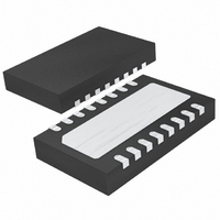
LTC4267CDHC-3#PBF Linear Technology, LTC4267CDHC-3#PBF Datasheet - Page 19

LTC4267CDHC-3#PBF
Manufacturer Part Number
LTC4267CDHC-3#PBF
Description
IC POE 802.3AF W/REG 16-DFN
Manufacturer
Linear Technology
Datasheet
1.LTC4267CGN-3PBF.pdf
(32 pages)
Specifications of LTC4267CDHC-3#PBF
Controller Type
Power over Ethernet Controller (POE)
Interface
IEEE 802.3af
Current - Supply
3mA
Operating Temperature
0°C ~ 70°C
Mounting Type
Surface Mount
Package / Case
16-DFN
Lead Free Status / RoHS Status
Lead free / RoHS Compliant
Voltage - Supply
-
Available stocks
Company
Part Number
Manufacturer
Quantity
Price
APPLICATIO S I FOR ATIO
Power Good Interface
The PWRGD signal is controlled by a high voltage, open-
drain transistor. The designer has the option of using this
signal to enable the onboard switching regulator through
the I
interface circuits for controlling the switching regulator
are shown in Figure 7.
In some applications, it is desirable to ignore intermittent
power bad conditions. This can be accomplished by in-
cluding capacitor C15 in Figure 7 to form a lowpass fi lter.
With the components shown, power bad conditions less
than about 200µs will be ignored. Conversely, in other
applications it may be desirable to delay assertion of
PWRGD to the switching regulator using C
as shown in Figure 7.
It is recommended that the designer use the power
good signal to enable the switching regulator. Using
PWRGD ensures the capacitor C1 has reached within
1.5V of the fi nal value and is ready to accept a load. The
LTC4267-3 is designed with wide power good hysteresis
to handle sudden fl uctuations in the load voltage and
current without prematurely shutting off the switching
regulator. Please refer to the Power-Up Sequencing of the
Application Information section.
Signature Disable Interface
To disable the 25k signature resistor, connect SIGDISA pin
to the V
high with respect to V
disable interface is shown in Figure 16, option 2. Note that
the SIGDISA input resistance is relatively large and the
threshold voltage is fairly low. Because of high voltages
present on the printed circuit board, leakage currents from
the V
ensure trouble-free operation, use high voltage layout
techniques in the vicinity of SIGDISA. If unused, connect
SIGDISA to V
TH
PORTP
/RUN or the P
PORTP
pin could inadvertently pull SIGDISA high. To
PORTN
pin. Alternately, SIGDISA pin can be driven
.
U
VCC
PORTN
U
pins. Examples of active-high
. An example of a signature
W
PVCC
U
or C17
Load Capacitor
The IEEE 802.3af specifi cation requires that the PD main-
tain a minimum load capacitance of 5µF (provided by C1
in Figure 11). It is permissible to have a much larger load
capacitor and the LTC4267-3 can charge very large load
capacitors before thermal issues become a problem. The
load capacitor must be large enough to provide suffi cient
energy for proper operation of the switching regulator.
However, the capacitor must not be too large or the PD
design may violate IEEE 802.3af requirements.
If the load capacitor is too large, there can be a problem
with inadvertent power shutdown by the PSE. Consider
the following scenario. If the PSE is running at –57V
(maximum allowed) and the PD has detected and powered
up, the load capacitor will be charged to nearly –57V. If
for some reason the PSE voltage is suddenly reduced to
–44V (minimum allowed), the input bridge will reverse
bias and the PD power will be supplied by the load capaci-
tor. Depending on the size of the load capacitor and the
DC load of the PD, the PD will not draw any power for
a period of time. If this period of time exceeds the IEEE
802.3af 300ms disconnect delay, the PSE will remove
power from the PD. For this reason, it is necessary to
ensure that inadvertent shutdown cannot occur.
Very small output capacitors (≤10µF) will charge very
quickly in current limit. The rapidly changing voltage at
the output may reduce the current limit temporarily, caus-
ing the capacitor to charge at a somewhat reduced rate.
Conversely, charging a very large capacitor may cause the
current limit to increase slightly. In either case, once the
output voltage reaches its fi nal value, the input current
limit will be restored to its nominal value.
The load capacitor can store signifi cant energy when fully
charged. The design of a PD must ensure that this energy
is not inadvertently dissipated in the LTC4267-3. The
polarity-protection diode(s) prevent an accidental short
LTC4267-3
19
42673f


