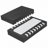
LTC4267CDHC-3#PBF Linear Technology, LTC4267CDHC-3#PBF Datasheet - Page 20

LTC4267CDHC-3#PBF
Manufacturer Part Number
LTC4267CDHC-3#PBF
Description
IC POE 802.3AF W/REG 16-DFN
Manufacturer
Linear Technology
Datasheet
1.LTC4267CGN-3PBF.pdf
(32 pages)
Specifications of LTC4267CDHC-3#PBF
Controller Type
Power over Ethernet Controller (POE)
Interface
IEEE 802.3af
Current - Supply
3mA
Operating Temperature
0°C ~ 70°C
Mounting Type
Surface Mount
Package / Case
16-DFN
Lead Free Status / RoHS Status
Lead free / RoHS Compliant
Voltage - Supply
-
Available stocks
Company
Part Number
Manufacturer
Quantity
Price
LTC4267-3
APPLICATIO S I FOR ATIO
on the cable from causing damage. However, if the V
pin is shorted to V
is charged, current will fl ow through the parasitic body
diode of the internal MOSFET and may cause permanent
damage to the LTC4267-3.
Maintain Power Signature
In an IEEE 802.3af system, the PSE uses the Maintain
Power Signature (MPS) to determine if a PD continues
to require power. The MPS requires the PD to periodically
draw at least 10mA and also have an AC impedance less
than 26.25k in parallel with 0.05µF . If either the DC current
is less than 10mA or the AC impedance is above 26.25k,
the PSE may disconnect power. The DC current must be
less than 5mA and the AC impedance must be above 2M
to guarantee power will be removed.
Selecting Feedback Resistor Values
The regulated output voltage of the switching regulator is
determined by the resistor divider across V
R2 in Figure 11) and the error amplifi er reference voltage
V
voltage can be calculated as:
In an isolated power supply application, V
by the designer’s choice of an external error amplifi er.
Commercially available error amplifi ers or programmable
shunt regulators may include an internal reference of 1.25V
or 2.5V. Since the LTC4267-3 internal reference and error
amplifi er are not used in an isolated design, tie the V
pin to PGND.
In a nonisolated power supply application, the LTC4267-3
onboard internal reference and error amplifi er can be
used. The resistor divider output can be tied directly to
the V
0.8V nominal.
20
REF
R2 = R1 • (V
. The ratio of R2 to R1 needed to produce the desired
FB
pin. The internal reference of the LTC4267-3 is
OUT
PORTP
– V
U
REF
inside the PD while the capacitor
U
)/V
REF
W
REF
is determined
OUT
U
(R1 and
PORTN
FB
Choose resistance values for R1 and R2 to be as large as
possible to minimize any effi ciency loss due to the static
current drawn from V
when V
input current from the output of the resistor divider to the
error amplifi er pin is less than 1%.
Error Amplifi er and Optoisolator Considerations
In an isolated topology, the selection of the external error
amplifi er depends on the output voltage of the switching
regulator. Typical error amplifi ers include a voltage refer-
ence of either 1.25V or 2.5V. The output of the amplifi er
and the amplifi er upper supply rail are often tied together
internally. The supply rail is usually specifi ed with a wide
upper voltage range, but it is not allowed to fall below the
reference voltage. This can be a problem in an isolated
switcher design if the amplifi er supply voltage is not prop-
erly managed. When the switcher load current decreases
and the output voltage rises, the error amplifi er responds
by pulling more current through the LED. The LED voltage
can be as large as 1.5V, and along with R
supply voltage to the error amplifi er. If the error amp does
not have enough headroom, the voltage drop across the
LED and R
causing a lock-up condition in the main loop. The switcher
will undershoot and not recover until the error amplifi er
releases its sink current. Care must be taken to select the
reference voltage and R
always has enough headroom. An alternate solution that
avoids these problems is to utilize the LT1431 or LT4430
where the output of the error amplifi er and amplifi er supply
rail are brought out to separate pins.
The PD designer must also select an optoisolator such
that its bandwidth is suffi ciently wider than the bandwidth
of the main control loop. If this step is overlooked, the
main control loop may be diffi cult to stabilize. The output
OUT
is in regulation, the error caused by the nonzero
LIM
may shut the amplifi er off momentarily,
OUT
LIM
, but just small enough so that
value so that the error amplifi er
LIM
, reduces the
42673f


