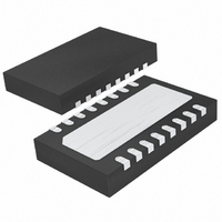
LTC4267CDHC-3#PBF Linear Technology, LTC4267CDHC-3#PBF Datasheet - Page 27

LTC4267CDHC-3#PBF
Manufacturer Part Number
LTC4267CDHC-3#PBF
Description
IC POE 802.3AF W/REG 16-DFN
Manufacturer
Linear Technology
Datasheet
1.LTC4267CGN-3PBF.pdf
(32 pages)
Specifications of LTC4267CDHC-3#PBF
Controller Type
Power over Ethernet Controller (POE)
Interface
IEEE 802.3af
Current - Supply
3mA
Operating Temperature
0°C ~ 70°C
Mounting Type
Surface Mount
Package / Case
16-DFN
Lead Free Status / RoHS Status
Lead free / RoHS Compliant
Voltage - Supply
-
Available stocks
Company
Part Number
Manufacturer
Quantity
Price
APPLICATIO S I FOR ATIO
If auxiliary power is applied directly to the LTC4267-3
switching regulator (bypassing the LTC4267-3 PD inter-
face), a different set of tradeoffs arise. In the confi guration
shown in option 2, the wall transformer does not need
to exceed the LTC4267-3 turn-on UVLO requirement;
however, it is necessary to include diode D9 to prevent
the transformer from applying power to the LTC4267-3
interface controller. The transformer voltage requirement
will be governed by the needs of the onboard switching
regulator. However, power priority issues require more
intervention. If the wall transformer voltage is below
the PSE voltage, then priority will be given to the PSE
power. The LTC4267-3 interface controller will draw power
from the PSE while the transformer will sit unused. This
confi guration is not a problem in a PoE system. On the
other hand, if the wall transformer voltage is higher than
the PSE voltage, the LTC4267-3 switching regulator will
draw power from the transformer. In this situation, it is
necessary to address the issue of power cycling that may
occur if a PSE is present. The PSE will detect the PD and
apply power. If the switcher is being powered by the wall
transformer, then the PD will not meet the minimum load
requirement and the PSE will subsequently remove power.
The PSE will again detect the PD and power cycling will
start. With a transformer voltage above the PSE voltage,
it is necessary to either disable the signature, as shown
in option 2, or install a minimum load on the output of the
LTC4267-3 interface to prevent power cycling.
The third option also applies power directly to the
LTC4267-3 switching regulator, bypassing the LTC4267-3
interface controller and omitting diode D9. With the
diode omitted, the transformer voltage is applied to the
LTC4267-3 interface controller in addition to the switching
regulator. For this reason, it is necessary to ensure that the
transformer maintain the voltage between 38V and 57V
to keep the LTC4267-3 interface controller in its normal
U
U
W
U
operating range. The third option has the advantage of
automatically disabling the 25k signature resistor when
the external voltage exceeds the PSE voltage.
Power-Up Sequencing the LTC4267-3
The LTC4267-3 consists of two functional cells, the PD
interface and the switching regulator, and the power up
sequencing of these two cells must be carefully considered.
The PD designer should ensure that the switching regulator
does not begin operation until the interface has completed
charging up the load capacitor. This will ensure that the
switcher load current does not compete with the load
capacitor charging current provided by the PD interface
current limit circuit. Overlooking this consideration may
result in slow power supply ramp up, power-up oscilla-
tion, and possibly thermal shutdown.
The LTC4267-3 includes a power good signal in the PD
interface that can be used to indicate to the switching
regulator that the load capacitor is fully charged and
ready to handle the switcher load. Figure 7 shows two
examples of ways the PWRGD signal can be used to
control the switching regulator. The fi rst example employs
an N-channel MOSFET to drive the I
the shutdown threshold (typically 0.28V). The second
example drives P
Employing the second example has the added advan-
tage of adding delay to the switching regulator start-up
beyond the time the power good signal becomes active.
The second example ensures additional timing margin at
start-up without the need for added delay components. In
applications where it is not desirable to utilize the power
good signal, suffi cient timing margin can be achieved
with R
to a delay of two to three times longer than the duration
needed to charge up C1.
START
and C
VCC
PVCC
below the P
. R
START
and C
VCC
LTC4267-3
TH
turn-off threshold.
PVCC
/RUN port below
should be set
27
42673f


