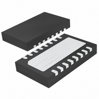
LTC4267CDHC-3#PBF Linear Technology, LTC4267CDHC-3#PBF Datasheet - Page 25

LTC4267CDHC-3#PBF
Manufacturer Part Number
LTC4267CDHC-3#PBF
Description
IC POE 802.3AF W/REG 16-DFN
Manufacturer
Linear Technology
Datasheet
1.LTC4267CGN-3PBF.pdf
(32 pages)
Specifications of LTC4267CDHC-3#PBF
Controller Type
Power over Ethernet Controller (POE)
Interface
IEEE 802.3af
Current - Supply
3mA
Operating Temperature
0°C ~ 70°C
Mounting Type
Surface Mount
Package / Case
16-DFN
Lead Free Status / RoHS Status
Lead free / RoHS Compliant
Voltage - Supply
-
Available stocks
Company
Part Number
Manufacturer
Quantity
Price
APPLICATIO S I FOR ATIO
In a nonisolated design, the LTC4267-3 incorporates an
internal error amplifi er where the I
a compensation point. In a similar manner, a series RC
network can be connected from I
shown in Figure 15. C
load and line transient response.
Selecting the Switching Transistor
With the N-channel power MOSFET driving the primary of
the transformer, the inductance will cause the drain of the
MOSFET to traverse twice the voltage across V
PGND. The LTC4267-3 operates with a maximum supply
of – 57V; thus the MOSFET must be rated to handle 114V
or more with suffi cient design margin. Typical transis-
tors have 150V ratings while some manufacturers have
developed 120V rated MOSFETs specifi cally for Power-
over-Ethernet applications.
The NGATE pin of the LTC4267-3 drives the gate of the
N-channel MOSFET. NGATE will traverse a rail-to-rail volt-
age from PGND to P
MOSFET provides a low “ON” resistance when switched
to P
handle the P
For high effi ciency applications, select an N-channel
MOSFET with low total gate charge. The lower total gate
charge improves the effi ciency of the NGATE drive circuit
and minimizes the switching current needed to charge
and discharge the gate.
Figure 15. Main Loop Compensation for a Nonisolated Design
VCC
as well as ensure the gate of the MOSFET can
VCC
supply voltage.
I
TH
U
C
/RUN
C
VCC
C
LTC4267-3
and R
. The designer must ensure the
U
R
PGND
Z
Z
are chosen for optimum
TH
W
TH
/RUN pin serves as
/RUN to PGND as
42673 F15
U
PORTP
and
Auxiliary Power Source
In some applications, it may be desirable to power the
PD from an auxiliary power source such as a wall trans-
former. The auxiliary power can be injected into the PD at
several locations and various trade-offs exist. Power can
be injected at the 3.3V or 5V output of the isolated power
supply with the use of a diode ORing circuit. This method
accesses the internal circuits of the PD after the isolation
barrier and therefore meets the 802.3af isolation safety
requirements for the wall transformer jack on the PD.
Power can also be injected into the PD interface portion of
the LTC4267-3. In this case, it is necessary to ensure the
user cannot access the terminals of the wall transformer
jack on the PD since this would compromise the 802.3af
isolation safety requirements.
Figure 16 demonstrates three methods of diode ORing
external power into a PD. Option 1 inserts power before
the LTC4267-3 interface controller while options 2 and
3 bypass the LTC4267-3 interface controller section and
power the switching regulator directly.
If power is inserted before the LTC4267-3 interface con-
troller, it is necessary for the wall transformer to exceed
the LTC4267-3 UVLO turn-on requirement and include a
transient voltage suppressor (TVS) to limit the maximum
voltage to 57V. This option provides input current limit
for the transformer, provides a valid power good signal,
and simplifi es power priority issues. As long as the wall
transformer applies power to the PD before the PSE, it
will take priority and the PSE will not power up the PD
because the wall power will corrupt the 25k signature. If
the PSE is already powering the PD, the wall transformer
power will be in parallel with the PSE. In this case, prior-
ity will be given to the higher supply voltage. If the wall
transformer voltage is higher, the PSE should remove the
line voltage since no current will be drawn from the PSE.
On the other hand, if the wall transformer voltage is lower,
the PSE will continue to supply power to the PD and the
wall transformer will not be used. Proper operation should
occur in either scenario.
LTC4267-3
25
42673f


