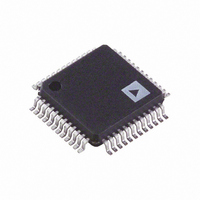
AD9951YSVZ Analog Devices Inc, AD9951YSVZ Datasheet - Page 21

AD9951YSVZ
Manufacturer Part Number
AD9951YSVZ
Description
IC DDS DAC 14BIT 1.8V 48-TQFP
Manufacturer
Analog Devices Inc
Specifications of AD9951YSVZ
Resolution (bits)
14 b
Master Fclk
400MHz
Tuning Word Width (bits)
32 b
Voltage - Supply
1.71 V ~ 1.96 V
Operating Temperature
-40°C ~ 105°C
Mounting Type
Surface Mount
Package / Case
48-TQFP Exposed Pad, 48-eTQFP, 48-HTQFP, 48-VQFP
Data Rate
25Mbps
Rf Ic Case Style
TQFP
No. Of Pins
48
Supply Voltage Range
1.8V To 3.3V
Operating Temperature Range
-40°C To +105°C
Msl
MSL 3 - 168 Hours
Ic Function
Direct Digital Synthesizer
Digital Ic Case Style
TQFP
Svhc
No SVHC (15-Dec-2010)
Rohs Compliant
Yes
Termination Type
SMD
Ic Generic Number
9951
Base Number
9951
Filter Terminals
SMD
Lead Free Status / RoHS Status
Lead free / RoHS Compliant
For Use With
AD9951/PCB - BOARD EVAL FOR AD9951
Lead Free Status / Rohs Status
Compliant
Available stocks
Company
Part Number
Manufacturer
Quantity
Price
Company:
Part Number:
AD9951YSVZ
Manufacturer:
AD
Quantity:
1 300
Company:
Part Number:
AD9951YSVZ
Manufacturer:
ADI
Quantity:
102
Company:
Part Number:
AD9951YSVZ
Manufacturer:
ADI
Quantity:
650
Company:
Part Number:
AD9951YSVZ
Manufacturer:
Analog Devices Inc
Quantity:
10 000
There are two phases to a communication cycle with the
AD9951. Phase 1 is the instruction cycle, which is the writing of
an instruction byte into the AD9951, coincident with the first
eight SCLK rising edges. The instruction byte provides the
AD9951 serial port controller with information regarding the
data transfer cycle, which is Phase 2 of the communication cycle.
The Phase 1 instruction byte defines whether the upcoming data
transfer is read or write and the serial address of the register
being accessed.
The first eight SCLK rising edges of each communication cycle
are used to write the instruction byte into the AD9951. The
remaining SCLK edges are for Phase 2 of the communication
cycle. Phase 2 is the actual data transfer between the AD9951
and the system controller. The number of bytes transferred
SCLK
SCLK
SCLK
SCLK
SDIO
SDIO
SDIO
SDIO
SDO
CS
CS
CS
CS
I
I
7
7
I
I
7
7
I
I
6
6
I
I
6
6
Figure 24. 2-Wire Serial Port Read Timing—Clock Stall High
INSTRUCTION CYCLE
INSTRUCTION CYCLE
I
INSTRUCTION CYCLE
I
INSTRUCTION CYCLE
Figure 22. 3-Wire Serial Port Read Timing–Clock Stall Low
5
5
I
I
5
5
Figure 23. Serial Port Write Timing–Clock Stall High
Figure 21. Serial Port Write Timing–Clock Stall Low
I
I
4
4
I
I
4
4
I
I
3
3
I
I
3
3
I
I
2
2
I
I
2
2
Rev. A | Page 21 of 28
I
I
1
1
I
I
1
1
I
I
0
0
I
I
0
0
D
D
O 7
during Phase 2 of the communication cycle is a function of the
register being accessed. For example, when accessing the Control
Function Register No. 2, which is three bytes wide, Phase 2 requires
that three bytes be transferred. If accessing the frequency tuning
word, which is four bytes wide, Phase 2 requires that four bytes
be transferred. After transferring all data bytes per the instruc-
tion, the communication cycle is completed.
At the completion of any communication cycle, the AD9951
serial port controller expects the next eight rising SCLK edges
to be the instruction byte of the next communication cycle. All
data input to the AD9951 is registered on the rising edge of
SCLK. All data is driven out of the AD9951 on the falling edge
of SCLK. Figure 21 through Figure 24 are useful in understand-
ing the general operation of the AD9951 serial port.
7
D
D
7
O 7
D
D
6
O 6
D
D
O 6
DATA TRANSFER CYCLE
DATA TRANSFER CYCLE
DATA TRANSFER CYCLE
DATA TRANSFER CYCLE
6
D
D
5
O 5
DON'T CARE
D
D
O 5
5
D
D
4
O 4
D
D
O 4
4
D
D
3
O 3
D
D
O 3
D
3
D
2
O 2
D
D
O 2
2
D
D
1
O 1
D
D
O 1
1
D
0
D
O 0
D
O 0
D
0
AD9951


