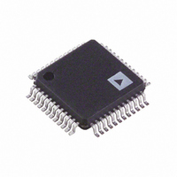
AD9951YSVZ Analog Devices Inc, AD9951YSVZ Datasheet - Page 23

AD9951YSVZ
Manufacturer Part Number
AD9951YSVZ
Description
IC DDS DAC 14BIT 1.8V 48-TQFP
Manufacturer
Analog Devices Inc
Specifications of AD9951YSVZ
Resolution (bits)
14 b
Master Fclk
400MHz
Tuning Word Width (bits)
32 b
Voltage - Supply
1.71 V ~ 1.96 V
Operating Temperature
-40°C ~ 105°C
Mounting Type
Surface Mount
Package / Case
48-TQFP Exposed Pad, 48-eTQFP, 48-HTQFP, 48-VQFP
Data Rate
25Mbps
Rf Ic Case Style
TQFP
No. Of Pins
48
Supply Voltage Range
1.8V To 3.3V
Operating Temperature Range
-40°C To +105°C
Msl
MSL 3 - 168 Hours
Ic Function
Direct Digital Synthesizer
Digital Ic Case Style
TQFP
Svhc
No SVHC (15-Dec-2010)
Rohs Compliant
Yes
Termination Type
SMD
Ic Generic Number
9951
Base Number
9951
Filter Terminals
SMD
Lead Free Status / RoHS Status
Lead free / RoHS Compliant
For Use With
AD9951/PCB - BOARD EVAL FOR AD9951
Lead Free Status / Rohs Status
Compliant
Available stocks
Company
Part Number
Manufacturer
Quantity
Price
Company:
Part Number:
AD9951YSVZ
Manufacturer:
AD
Quantity:
1 300
Company:
Part Number:
AD9951YSVZ
Manufacturer:
ADI
Quantity:
102
Company:
Part Number:
AD9951YSVZ
Manufacturer:
ADI
Quantity:
650
Company:
Part Number:
AD9951YSVZ
Manufacturer:
Analog Devices Inc
Quantity:
10 000
When the CFR1<3> bit is 0 and the PWRDWNCTL input pin is
high, the AD9951 is put into a fast recovery power-down mode.
In this mode, the digital logic and the DAC digital logic are
powered down. The DAC bias circuitry, PLL, oscillator, and
clock input circuitry is NOT powered down.
When the CFR1<3> bit is high, and the PWRDWNCTL input
pin is high, the AD9951 is put into the full power-down mode.
In this mode, all functions are powered down. This includes the
DAC and PLL, which take a significant amount of time to
power up.
When the PWRDWNCTL input pin is high, the individual
power-down bits (CFR1<7>, <5:4>) are invalid (Don’t Care)
and unused. When the PWRDWNCTL input pin is low, the
individual power-down bits control the power-down modes of
operation.
Note that the power-down signals are all designed such that a
Logic 1 indicates the low power mode and a Logic 0 indicates
the active or powered up mode.
Table 8. Power-Down Control Functions
Control
PWRDWNCTL = 0 CFR1<3> Don’t Care
PWRDWNCTL = 1 CFR1<3> = 0
PWRDWNCTL = 1 CFR1<3> = 1
Mode Active
Software Control
External Control,
Fast Recovery Power-Down Mode
External Control,
Full Power-Down Mode
Rev. A | Page 23 of 28
Table 8 indicates the logic level for each power-down bit that
drives out of the AD9951 core logic to the analog section and
the digital clock generation section of the chip for the external
power-down operation.
Layout Considerations
For the best performance, the following layout guidelines
should be observed. Always provide the analog power supply
(AVDD) and the digital power supply (DVDD) on separate
supplies, even if just from two different voltage regulators
driven by a common supply. Likewise, the ground connections
(AGND, DGND) should be kept separate as far back to the
source as possible (i.e., separate the ground planes on a loca-
lized board, even if the grounds connect to a common point in
the system). Bypass capacitors should be placed as close to the
device pin as possible. Usually, a multitiered bypassing scheme
consisting of a small high frequency capacitor (100 pF) placed
close to the supply pin and progressively larger capacitors (0.1 µF,
10 µF) further away from the actual supply source works best.
Description
Digital Power-Down = CFR1<7>
DAC Power-Down = CFR1<5>
Input Clock Power-Down = CFR1<4>
Digital Power-Down = 1’b1
DAC Power-Down = 1’b0
Input Clock Power-Down = 1’b0
Digital Power-Down = 1’b1
DAC Power-Down = 1’b1
Input Clock Power-Down = 1’b1
AD9951


