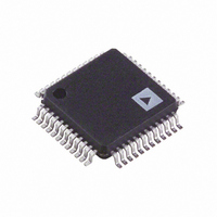
AD9954YSVZ Analog Devices Inc, AD9954YSVZ Datasheet - Page 16

AD9954YSVZ
Manufacturer Part Number
AD9954YSVZ
Description
IC DDS DAC 14BIT 1.8V 48-TQFP
Manufacturer
Analog Devices Inc
Datasheet
1.AD9954YSVZ-REEL7.pdf
(40 pages)
Specifications of AD9954YSVZ
Resolution (bits)
14 b
Master Fclk
400MHz
Tuning Word Width (bits)
32 b
Voltage - Supply
1.71 V ~ 1.96 V
Operating Temperature
-40°C ~ 105°C
Mounting Type
Surface Mount
Package / Case
48-TQFP Exposed Pad, 48-eTQFP, 48-HTQFP, 48-VQFP
Data Rate
25Mbps
Rf Ic Case Style
TQFP
No. Of Pins
48
Supply Voltage Range
1.71V To 1.89V, 3.135V To 3.465V
Operating Temperature Range
-40°C To +105°C
Msl
MSL 3 - 168 Hours
Termination Type
SMD
Rohs Compliant
Yes
Filter Terminals
SMD
Lead Free Status / RoHS Status
Lead free / RoHS Compliant
For Use With
AD9954/PCBZ - BOARD EVAL FOR 9954
Lead Free Status / RoHS Status
Lead free / RoHS Compliant, Lead free / RoHS Compliant
Available stocks
Company
Part Number
Manufacturer
Quantity
Price
Company:
Part Number:
AD9954YSVZ
Manufacturer:
ADI
Quantity:
210
Company:
Part Number:
AD9954YSVZ
Manufacturer:
Analog Devices Inc
Quantity:
10 000
Part Number:
AD9954YSVZ
Manufacturer:
ADI/亚德诺
Quantity:
20 000
Company:
Part Number:
AD9954YSVZ-REEL7
Manufacturer:
UBR
Quantity:
6 000
Company:
Part Number:
AD9954YSVZ-REEL7
Manufacturer:
Analog Devices Inc
Quantity:
10 000
AD9954
Manual Shaped On-Off Keying Mode Operation
When configured for manual shaped on-off keying, the
content of the ASFR sets the scale factor for the data path.
MODES OF OPERATION
Single-Tone Mode
In single-tone mode, the DDS core uses a static tuning word.
Whatever value is stored in FTW0 is supplied to the phase
accumulator. This value can only be changed manually by
writing a new value to FTW0 and then by issuing an I/O update.
Phase adjustments are made using the phase offset register.
RAM-Controlled Modes of Operation
Three important points apply to the RAM-controlled modes:
The user must ensure that the beginning address is lower
Changing profiles or issuing an I/O update automatically
Setting the RAM destination bit true such that the RAM
The AD9954 offers five modes of RAM-controlled operation
(see Table 7).
Table 7. RAM Modes of Operation
RSCW<7:5> (Binary)
000
001
010
011
100
101, 110, 111
Direct Switch Mode
Direct switch mode enables frequency shift keying (FSK) or
phase shift keying (PSK) modulation. The AD9954 is
programmed for direct switch using the RAM enable bit
(CFR1<31>) and programming the RAM segment mode
control bits of each desired profile to 000(b). This mode simply
reads the RAM contents at the RAM segment beginning
address for the current profile. No address ramping occurs in
this mode.
than the final address.
terminates the current sweep and starts the next sweep, unless
otherwise stated.
output drives the phase offset adder is valid. While the
sections that follow describe frequency sweeps, phase
sweep operation is also available. The RAM destination bit
(CFR1<30>) controls whether the RAM output drives the
phase accumulator (frequency) or the phase offset adder
(phase).
Mode
Direct Switch
Ramp Up
Bidirectional
Ramp
Continuous
Bidirectional
Ramp
Continuous
Recirculation
Invalid mode
Notes
No sweeping, profiles
valid, no dwell ignored
Sweeping, profiles valid,
no-dwell valid
Sweeping, PS0 is a
direction control pin,
no-dwell ignored
Sweeping, profiles valid,
no-dwell ignored
Sweeping, profiles valid,
no-dwell ignored
Default to direct switch
Rev. B | Page 16 of 40
To perform 4-tone shift keying, the user programs each RAM
segment control word for direct switch mode and a unique
beginning address value. Program the RAM enable and RAM
destination bits (CFR1<31:30>) to enable the RAM and direct
the RAM output to be the FTW (FSK) or the POW (PSK). The
PS1 and PS0 inputs are the 4-tone FSK/PSK data inputs. When
the profile is changed, the data stored at the new profile is
loaded into either the phase accumulator (FSK) or the phase
offset adder (PSK). When set for PSK, Bits<17:0> of the RAM
output are unused when the RAM destination bit is set. Two-
tone shift keying only uses one profile pin.
Ramp-Up Mode
Ramp-up mode, in conjunction with the segmented RAM
capability, allows up to four different sweep profiles to be
programmed into the AD9954. The AD9954 is programmed
for ramp-up mode by enabling the RAM using the RAM enable
bit (CFR1<31>) and programming the RAM mode control bits
of each profile to be used to 001(b).
When a sweep is initiated (via an I/O update or change in
profile bits), the RAM address generator loads the RAM
segment beginning address bits of the current RSCW, driving
the RAM output from this address, and the ramp rate timer
loads the RAM segment address ramp rate bits. When the ramp
rate timer finishes a cycle, the RAM address generator increments
to the next address, the timer reloads the ramp rate bits and
begins a new countdown cycle. This sequence continues until
the RAM address generator has incremented to an address
equal to the RAM segment final address bits of the current
RSCW. At this point, the next state is dependent upon whether
no-dwell mode is active. See the no-dwell bit (CFR1<2>) in the
register maps (see Table 12 and Table 13).
In this mode, asymmetrical FSK modulation can be implemented
by configuring the RAM for two segments, and using the PS0
pin as the data input.
Bidirectional Ramp Mode
Bidirectional ramp mode allows the AD9954 to offer a
symmetrical sweep between two frequencies using the PS0
signal as the control input. The AD9954 is programmed for
bidirectional ramp mode using the RAM enable bit (CFR1<31>)
and programming the RAM segment mode control bits of each
desired profile to 010(b). PS1 input is ignored; the PS0 input is
the ramp direction indicator. The memory is not segmented,
using only one beginning and one final address. The address
registers for controlling RAM are located in the RAM segment
control word (RSCW) associated with Profile 0.


